PCB vs PCBA: Understanding the Key Differences and Applications
Table of Contents
ToggleHow Do PCB and PCBA Relate to Each Other?
Introduction
In the world of electronics manufacturing, understanding the distinction between a PCB (Printed Circuit Board) and a PCBA (Printed Circuit Board Assembly) is fundamental. Both are often used interchangeably by beginners, but they play very different roles in the electronics manufacturing process. For engineers, designers, and businesses, knowing the differences in detail between a blank PCB and a fully assembled PCBA is essential to success—whether you’re involved in prototyping or mass-producing sophisticated electronic devices.
This guide explores the key differences between PCB and PCBA, delving deep into materials, fabrication, assembly, applications, and why both have become indispensable in electronics. You’ll learn how a PCB, which is a bare board at first, becomes a PCBA ready for integration into final products, and how to choose the right PCB and PCBA solutions for your needs.
What is a PCB? (Printed Circuit Board)
Definition and Significance of PCBs
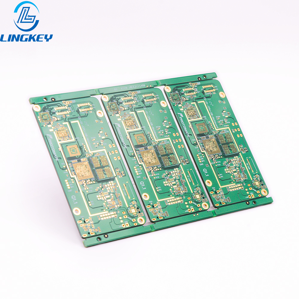
PCB stands for printed circuit board.At its most basic, a PCB is a bare circuit made of a non-conductive substrate (usually FR4) with a thin layer of copper etched onto it to form the circuit paths. It’s the foundation of electronics manufacturing, providing physical support and electrical connections for various components.
A PCB is a bare board, so it doesn’t contain any electronic components—it’s simply a blank circuit board with copper traces, mounting points, and drilled holes for assembly. PCBs provide a reliable and cost-effective solution for organizing and connecting components within electronic devices and are one of the most critical steps in electronic device manufacturing.
Key Components of a PCB
- Substrate (PCB Material):The most common is FR4 (fiberglass), but other insulating materials, such as CEM-1 and polyimide, are also available. These materials are selected primarily for factors such as mechanical strength and heat resistance.
- Copper Traces:Thin layers of copper form pathways, linking various pads on the surface of the PCB.
- Solder Mask:A protective, colored layer that prevents oxidation and accidental solder bridging between pads.
- Silkscreen:Printed labels indicating component placement, reference designators, or logos.
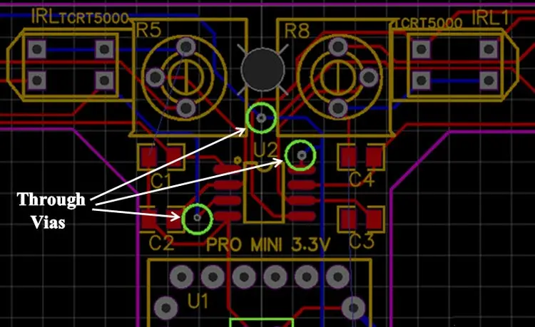
- Holes and Vias:Holes drilled into the PCB (for through-hole mounting and layer interconnection) are pivotal in multi-layer PCBs.
- PCB Pads:Small exposed copper areas used to solder components onto the PCB during assembly.
Types of PCBs
- Single-Layer PCB:The simplest type of PCB—a simple PCB with copper traces on one side, primarily used for low-cost or low-complexity electronic circuit designs.
- Multi-layer PCB:Containing four or more stacked layers, they enable denser and more complex circuits and are ubiquitous in many electronic products.
- Rigid PCB:Maintain a fixed shape and are most common in traditional PCB applications.
- Rigid-flex PCBs:A hybrid PCB that combines rigidity and flexibility, suitable for highly complex designs.
PCB Fabrication Process
PCB manufacturing begins with circuit design, typically using CAD layout tools to generate Gerber files detailing each layer. The process includes:
- Material Cutting: Determines the dimensions of the selected PCB material.
- Lamination: Bonds the copper sheets to the substrate.
- Inner Layer Routing and Etching: Etches the circuit pattern into the copper board.
- Drilling: Drills precision holes for component leads or vias.
- Plating: Creates plated-through holes (PTHs) for electrical connections between layers.
- Solder Mask and Silkscreen Application: Protects the board’s copper and aids assembly.
- Surface Finish: PCBs may be treated with HASL, ENIG, silver, or other materials to improve solderability.
- Testing and Inspection: This includes electrical testing and automated inspection (AOI) to confirm circuit continuity.
Common Applications of PCBs
PCBs are used in nearly every device in modern electronics, from consumer products like smartphones to critical applications in automotive, aerospace, industrial control, medical technology, and the Internet of Things. Choosing the right PCB—whether single-layer, multi-layer, rigid, flexible, or rigid-flex—is crucial for functionality, size, and reliability.
What is a PCBA? (Printed Circuit Board Assembly)
Definition and Purpose of PCBA
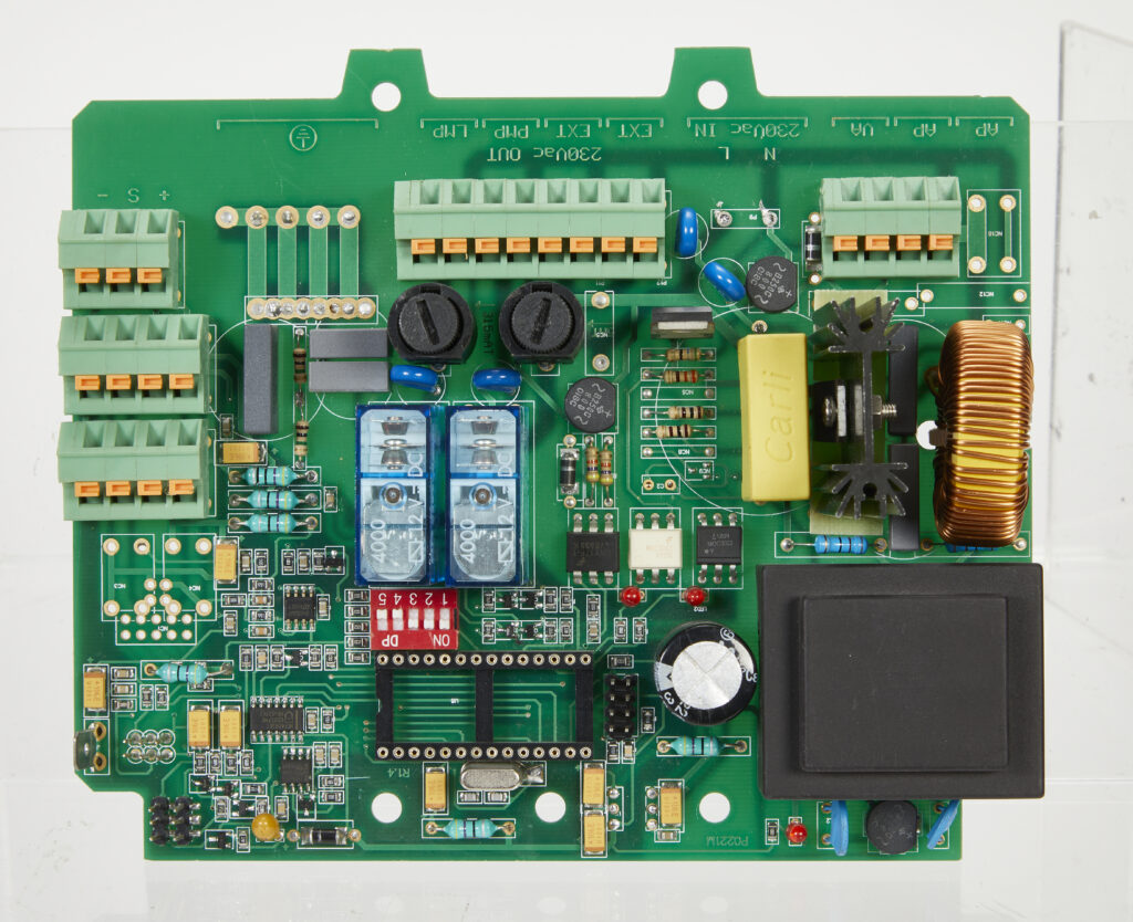
A PCBA (Printed Circuit Board Assembly) refers to a PCB (printed circuit board) with all components already assembled. A printed circuit assembly (PCB) can be directly assembled into an electronic device. While a PCB is a blank circuit board, a PCBA is a fully assembled, functional finished circuit capable of realizing the product’s functionality.
A PCBA is a complete, fully functional assembly that sits at the heart of a product, encompassing everything from power transmission to data processing. In the electronics industry, a PCBA is the final electronic circuit that can be used in a larger system.
PCBA Composition
A PCBA consists of the following components:
PCB substrate: A blank PCB that serves as the foundation.
Electronic components: Integrated circuits (ICs), capacitors, and resistors—selected based on the circuit design.
Solder: Bonds the components to the PCB pads.
Adhesive and traces: Ensure stability and continuous circuit continuity.
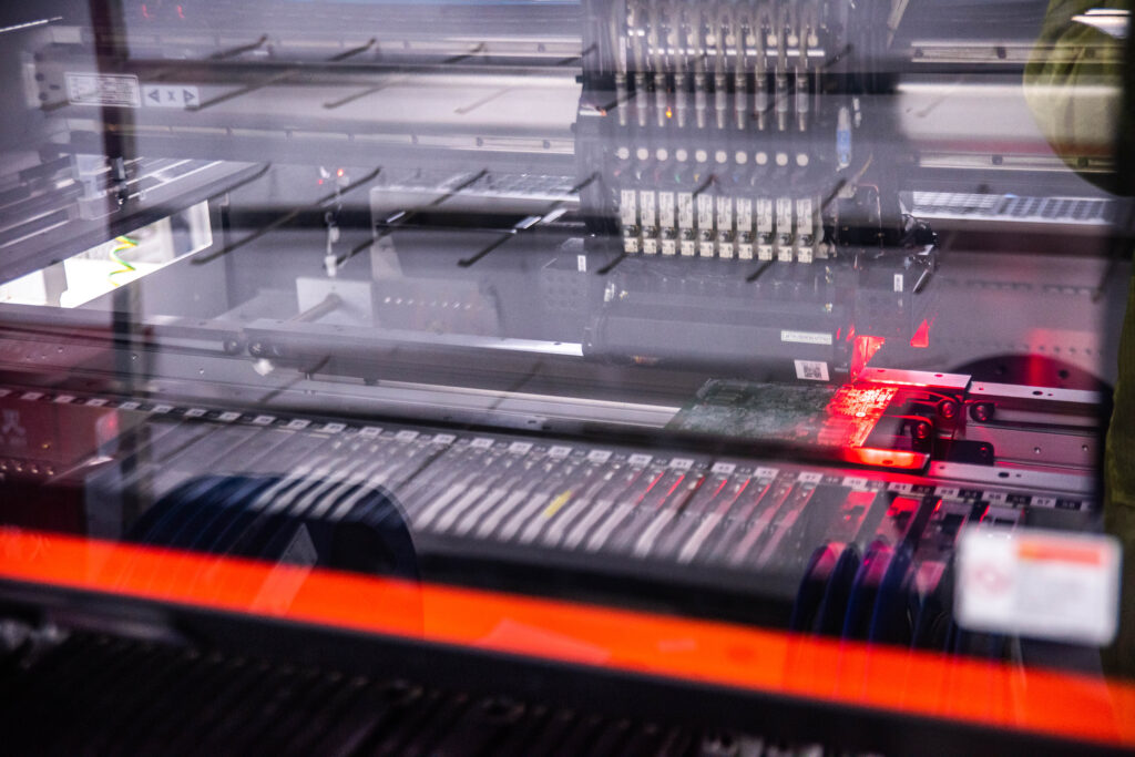
PCBA Manufacturing Process
The PCB assembly process involves several steps:
- Component Sourcing:All electronic components are collected and listed on a form (BOM).
- Solder Paste Application:Solder paste is applied to the PCB pads using a stencil.
- Component Placement:High-speed pick-and-place machines or manual placement for some parts.
- Soldering:
- SMT (Surface Mount Technology):Automated placement and reflow soldering.
- THT (Through-Hole Technology):Leads inserted into holes in the PCB; wave soldering or hand soldering.
5. Inspection and Testing:AOI, X-ray, and FCT ensure component placement accuracy and functional performance.
Main PCB Assembly Methods
- Surface Mount Technology (SMT):Enables compact, high-density designs crucial for multi-layer PCBA.
- Through-Hole Technology (THT):Ideal for components needing strong mechanical anchoring.
- Hybrid Methods:Combining SMT and THT, used frequently in specialized or high-reliability assemblies.
PCBA Testing and Quality Assurance
Quality inspection during and after assembly is crucial. The following processes are performed:
Automated Optical Inspection (AOI):Quickly detects placement and soldering errors.
n-Circuit Test (ICT):Tests for shorts, opens, and proper orientation of electronic components.
- Functional Circuit Test (FCT):Verifies the board’s overall operation and logic functionality according to the design.
- Flying Probe Test:Ideal for prototype or low-volume runs, checking continuity and connections without fixed test fixtures.
- Aging/Burn-in and Environmental Stress Testing:Ensures reliability under harsh conditions, uncovering latent failures before deployment.
PCBA is the final functional component that realizes the product, so rigorous testing is crucial to the electronic product manufacturing process. It ensures that each assembled circuit board meets the specifications and reliability standards required by consumers and regulations.
PCB vs PCBA: Key Differences
Below is a concise table showing the key differences between PCB and PCBA, clarifying the stages in electronics manufacturing:
Aspect | PCB (Printed Circuit Board) | PCBA (Printed Circuit Board Assembly) |
Definition | Blank PCB – the basic substrate with copper traces; a bare board | PCB with components soldered, tested, and ready to use |
Stage | Early stage in electronics manufacturing | Later, value-added stage (finished and functional) |
Function | Provides structure and physical connections | Implements intended electronic circuit and function |
Fabrication | PCB fabrication, drilling holes in the pcb, making copper traces | Assembles and solders components, forming the complete PCBA |
Components | None (PCB is a blank circuit) | All electronic circuit components included |
Assembly Process | Not required for PCB | Requires PCB assembly process: SMT, THT, hybrid |
Cost | Lower — cost of material and fabrication only | PCBA is more expensive due to components, labor, and QA |
Testing | Basic tests: electrical continuity, AOI | Extensive: AOI, ICT, FCT, environmental testing |
Use Case | Prototyping, education, initial design | Fully functional assemblies used in final products |
Production Lead Time | Shorter | Longer, due to assembly/testing/state complexity |
Explained Distinctions
A PCBA and PCB differ in function and position within the electronics manufacturing chain, respectively. A PCB is simply an unassembled circuit board marked only with text and pads for mounting components; on the other hand, a PCBA contains fully assembled electronic circuitry featuring components like microchips, resistors, capacitors all meticulously assembled onto its surface for soldering onto it.
The PCBA is the heart of any electronic device. It’s the final, tested, and ready-to-use circuit board that integrates the design intent of a printed circuit with the actual hardware. While a PCB can be a simple board for educational, testing, or prototyping purposes, the PCBA is the finished product found in all electronic devices, from smartphones to medical devices.
How Do PCB and PCBA Relate to Each Other?
The PCB is the foundation of the PCB. It is manufactured by a PCB manufacturer based on custom design files (Gerber data) and specifications. The blank PCB then enters the assembly stage, where components are soldered to the PCB using SMT, THT, or a hybrid of the two technologies.
As each process is completed – design, PCB manufacturing, component procurement, placement, soldering, testing – a blank PCB will gradually become a complete PCB. Understanding this process can help engineers, designers and procurement teams better optimize the product development cycle.
Applications of PCB and PCBA in Different Industries
In today’s era of popular electronic products, PCB and PCBA have become an indispensable part. Their application areas include:
Consumer Electronics: High-density multilayer PCBs power devices ranging from smart TVs to wearable fitness trackers.
Automotive Electronics: Both rigid and rigid-flex PCBs enable compact, robust control modules and real-time monitoring systems.
Industrial Controls: Durable PCB and PCBA solutions withstand the harsh factory environments found in automation equipment and robotics.
Medical Devices: From diagnostic equipment to implantable electronics, PCBAs meet stringent reliability and cleanliness standards.
Telecommunications and Computing: High-speed multilayer PCBs and PCBA solutions power routers, servers, and network switches.
Aerospace/Defense: Advanced design, robust PCB materials, and flawless assembly ensure functionality even under extreme conditions.
IoT Devices: The ongoing trend toward miniaturization means that low-cost PCBs, flexible PCBs, and compact single- or double-sided PCBs are essential for connectivity and remote monitoring。
Manufacturing Processes Compared: PCB vs PCBA
PCB Fabrication Workflow
PCB fabrication consists of several critical stages:
- Design and Gerber Files: Convert Gerber files to manufacturing files.
- Material Selection: Select the appropriate PCB material based on performance and cost.
- Image Transfer and Etching: Create copper traces, pads, and ground planes.
- Drilling: Create holes for component leads and vias on the PCB.
- Electroplating: Deposit copper in vias and on the surface as needed.
- Solder Mask and Silkscreen: Add protective layers and labels.
- Testing and Inspection: AOI and electrical testing ensure circuit continuity and accuracy.
PCBA Manufacturing Workflow
The assembly of a PCB into a fully functional PCBA includes:
- Component Sourcing:Reliable supply chain management is vital, as delays in parts can halt production.
- Stencil Printing (Solder Paste Application):Solder paste is applied to the necessary PCB pads.
- Pick-and-Place:Mounting of electronic components onto the board surface.
- Soldering:SMT for compact, automated production; THT for robustness; or hybrid for flexibility.
- Inspection:AOI and X-ray for verifying solder joints and placements.
- Functional Testing:Ensuring assembled boards perform as specified.
- Final QA:Cleaning, packaging, and prep for delivery—turnkey PCBA services can handle this entire workflow.
Choosing PCB vs PCBA for Your Project
When should you select just a PCB versus a fully assembled PCBA?
PCB (Printed Circuit Board):
- Ideal for in-house prototyping or when manual, custom assembly is planned.
- Useful during the early design and test phase when rapid iterations on a blank PCB are required.
- Costs less and provides flexibility but has no electrical function on its own.
PCBA (Printed Circuit Board Assembly):
- Required when you need a pcb with componentssoldered and tested, ready for system integration.
- Essential for volume products, pilot runs, or any application requiring repeatable reliability.
- While PCBA is more expensivedue to additional labor, testing, and component costs, it provides a fully assembled PCBA—invaluable in reducing errors, ensuring quality, and speeding up time-to-market.
Selecting a Reliable PCB/PCBA Manufacturer
Qualities to Look For
- Proven track record and portfolio in your target application fields.
- Capability with advanced PCB types—rigid, flexible, rigid-flex, multi-layer PCB, single-layer PCB.
- Transparency and expertise in both pcb fabricationand pcb assembly process.
- Adherence to industry certifications such as ISO 9001, IPC-A-610, and RoHS.
- Robust supply chain and lead time management (critical for complex, multi-layer PCBA orders).
- Strong quality control and after-sales support.
- Offers “turnkey PCBA” solutions, handling every stage—from sourcing and assembly to testing and fulfillment.
Common Challenges & Solutions
- Design Handover:Provide complete Gerber files, BOM, and assembly notes to ensure manufacturing accuracy.
- Quality Assurance:Insist on thorough inspection and transparent documentation.
- Lead Time:Opt for manufacturers with reliable sourcing and fast turnaround to keep projects on track.
Future Trends in PCB and PCBA Technology
The electronics industry is rapidly evolving:
- Ultra-high density, miniaturized PCBs and multi-layer PCBA
- Lead-free, eco-friendly, and sustainable materials.
- Greater automation, robotic pick-and-place, and smart DFM tools in the pcb assembly process.
- Expansion of low-cost PCB options for rapid prototyping and IoT.
- AI-powered inspection, predictive analytics, and real-time QMS in large-scale electronics manufacturing.
Conclusion
PCBAs and PCBs differ more than just semantically; each plays its own important role in electronics production, with unique materials, methods, and challenges associated with each. A PCB acts as the silent backbone for every electronic circuit while PCBA is the final assembled board that brings products or ideas to life.
Understanding the relationship between PCB and PCBA can optimize the product cycle during design, procurement and production. In the production process, the appropriate PCB material, assembly method and strict quality control all determine the quality of the final product.
As the PCB manufacturing industry continues to develop, requirements such as miniaturization, automation, and multi-layer complexity are constantly increasing. Working with Lingkey’s many years of experience in the PCB and PCB industry to provide powerful, flexible and turnkey PCBA solutions is not just a suggestion, but also the key to innovation and reliability.
If you’re ready to transform your design from a blank PCB into a game-changing electronic circuit, choose Lingkey, a partner with extensive experience, comprehensive capabilities, and a commitment to quality every step of the way, from prototyping to delivery of your next fully assembled PCBA.
")
")


")
")
")


