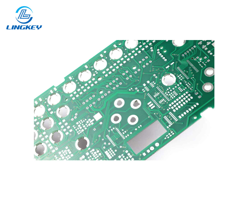
Through Hole
A through hole on a PCB is a hole drilled from the top to the bottom of the PCB. These holes are used for mounting electronic components. Component leads are inserted into the through hole on the PCB and soldered to pads on the other side either manually (by hand placement) or using an automatic insertion mounter.
Through Hole Classifications
1. Plated Through Hole (PTH)
The hole wall is electroplated to form a conductive layer, connecting electrical signals and used for soldering plug-in components to the circuit board layer.
2. Non-Plated Through Hole (NPTH)
The hole wall is not plated with copper and is typically used for mechanical positioning or screw fixing.
Characteristics of Through Hole
item | explanation |
Whether it runs through the entire board | The through hole goes all the way from the top layer to the bottom layer |
Number of connection layers | All layers can be connected (top, inner, bottom) |
cost | Simple processing technology and low cost |
reliability | High mechanical strength and strong connection reliability |
Space occupancy | Occupies more PCB surface area, which is not conducive to high-density design |
Advantages of Through-Hole Connections
1. High Mechanical Strength and Secure Connections
Component pins pass through the circuit board through through-holes and are soldered in place on the other side, creating a double-sided connection. This provides a more secure connection to the circuit board and is ideal for assembling larger or heavier components.
2.High Soldering Reliability
Through-hole solder joints are typically larger, allowing the solder to fully encapsulate the pins, resulting in higher soldering strength.
3.Excellent electrical conductivity
Copper plating on the hole wall allows for stable electrical continuity between layers, allowing for high current carrying capacity.
4. Low Cost
Through-hole processing equipment is widely available, easy to operate, and the manufacturing cost is relatively stable.
Disadvantages of Through-Hole Vias
1. They Take Up Large Space, Impacting Wiring Density
Through-hole vias must penetrate from the top layer to the bottom layer, occupying wiring space and hindering high-density wiring designs.
2. Unsuitable for high-density, miniaturized designs
As electronic products move toward thinner, lighter, and smaller designs, through-hole processes are unable to meet these demands. Compared to blind and buried vias, through-hole processes waste space.
3.Not conducive to automated assembly
Through-hole mounting is typically used for plug-in components, requiring manual insertion or wave soldering, which is less efficient than fully automated SMT assembly lines.
4. Board Thickness Limitations
For thick boards, mechanical drilling takes longer, causes greater board wear, and increases the risk of misalignment.
5.High drilling precision requirements.
Strict hole diameter tolerances are essential, otherwise poor welding or abnormal conduction may occur.
