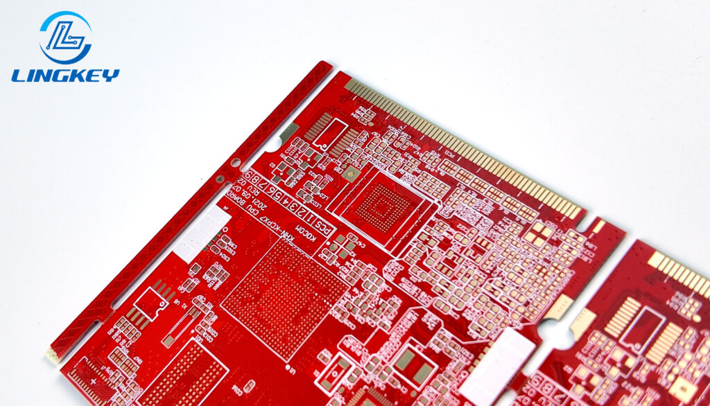
Gold Finger
There is a series of gold-colored conductive pads or fingers on one side of computer memory modules and graphics cards, whose rows are aligned with one another between which data can be transmitted. It looks like fingers and the color is golden which led to the name of “gold fingers”. They may also be called edge connectors.
Gold fingers are thin layer of gold plating at the end of the fingers of a PCB. They act as a PCB connector to the rest of your system and allow for signal or command transmission reliability. Besides, gold plating also acts as a protection for the edges of the circuit board.
Egde connector
Gold fingers and edge connectors are often confused, but they serve different functions:
Gold Fingers (Edge Fingers) – These are gold plated contact pads at
Edge Connector: It’s the plug that slides on the gold fingers.
Edge connectors are usually constructed from plastic or metal and have one or more rows of gold plated metal contacts, designed to accept gold plated contacts known as fingers. They offer a reliable mechanical plug-in connection and are utilized to connect the circuit board to other modules or external devices through which the data of circuit board can be shared or electrical signals can be exchanged. Some typical ones are expansion card slots, module sockets and alike interfaces.
Gold Fingers vs. Edge Connectors
Utility: Gold fingers are used to interface a PCB to peripherals or the motherboard for data transfer through USB and storage cards. Edg connectors are in computers as expansion slots enables connection of PCIe, PCI and AGP cards to the system bus).
Location: Gold fingers are on the edge of a board, but you can put an edge connector at any location on the PCB.
Packaging: Gold plating fingers are coated with gold to get better conductivity and longer-life. They are hot-pluggable. Although edge connectors themselves are surrounded by some sort of a thermoplastic enclosure with one side of the enclosure open and the pins are running along the edge.
Construction:Gold fingers are made of solder pads. They are formed after the solder mask production and need further milling in order to have chamfered edges. Conversely, edge connectors take the form of pins which are inserted and soldered into Through-Holes.
Application: Gold fingers are useful in applications where the connection is made a lot and taken apart a lot. With repeated insertion and removal of gold fingers, reliable electrical connections can be made without substantially damaging or wearing the connector or contact points. On the contrary, edge connectors are usually fixed once inserted in the board, and not so easy to take out and change.
Cost: Gold fingers are more expensive to manufacture as they need to be plated with gold. In contrast, edge connectors profess less cost, as they are commonly produced from plastic or metal materials.
Surface treatment methods for PCB gold fingers
Electroplated Nickel Gold: Electroplated nickel gold is commonly applied at thicknesses of 3–50µ” on the gold fingers of PCBs that are subject to frequent plugging/unplugging or mechanical abrasion. It has good electrical conductivity, is resistant to oxidation and has good wear resistance. However, gold plating is expensive, so it is usually applied for butter plating, such as gold fingers.
Immersion Gold: Generally at a thickness of 1 µ” up to 3 µ”, immersion gold is much applied to high precision PCBs with features like keypads, ic bonding or bga etc. It offers better conductivity, surface planarity and solder ability. For gold finger PCB which no need high wear resistance,whole board immersion gold can be considered as best economic option compare with electroplated gold. The tone of the gold in immersion gold is golden yellow.
Goldfinger category
Gold fingers can be categorized into three types: normal gold fingers (flush gold fingers), intermittent gold fingers (segment gold fingers), and emo gold fingers (jagged gold fingers).
Normal gold-fingers (Flush gold-fingers):same-size rectangular solder pads arranged neatly at the edge of the board. They are used for physical connections in network cards, graphics cards, and the like.
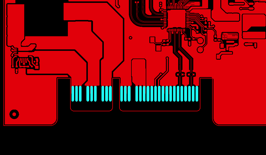
Divided gold fingers (disjunct gold fingers): at the edge of the PCB, the length of each rectangular solder pad is different and a front section is separated.
Irregular gold fingers (long - short fingers): the length of the rectangular pads along the PCB varies and they are found at the edge of the PCB.
They are frequently employed for physical connections in memory sticks, USB drives, and card readers, among other similar products.
Design Rules for Gold Fingers
- The distance between the gold fingers and the PCB board outline should be at least 0.5mm.
- Within 1mm of the gold fingers there should be no SMD parts, plated holes, or solder pads.
- All inner layers inside the gold fingers are subjected to copper removal so that during chamfering, there is no exposure of copper. Usually the width of copper removal should be more than It is performed either as full-finger or half-finger copper removal. PcIe designs there are signs All copper within the gold fingers should be removed. Copper removal underneath the fingers also effects into reducing the impedance mismatch between the gold fingers and impedance controlled traces, which adds additional ESD protection benefits too.
- No gold finger should be longer than 40mm.
- Keep away from soldermask or silkscreen printing from the gold fingers.
- In order to improve wear-resistance of gold fingers which is typically hard gold plated.
- Gold fingers must have a shoebox shaped opening or a continuous solder mask opening without steel mesh for the pins. In the PCB design gold fingers must have a continuous solder mask opening under no circumstances steel mesh is allowed for the pins.
- Gold fingers should be chamfered and usually it is 45°. Other angles like 20° or 30° are also available. No chamfers are applied on the PCB design of gold fingers, that’s a problem. In the image below, the arrow indicates a 45°
