Smt Surface Mount Technology
SMT (Surface Mount Technology) is an electronics assembly technique that places electronic components directly on the surface of a printed circuit board (PCB). Due to its low cost and high quality efficiency, SMT has largely replaced through-hole mounting technology.
Advantages of SMT patch processing
- Using automated equipment can complete patching more efficiently, improving patching efficiency compared to traditional through-hole technology.
- In a limited PCB space, a large number of micro components can be mounted, and components can also be placed on both sides of the PCB, with more connections per component. Higher component density.
- The resistance and inductance at the connection are relatively low, which can reduce unnecessary RF signals and make the electronic product signal transmission efficient and have higher performance.
- Reduce the number of drilling holes, reduce costs and save time
- Better EMC performance (lower radiated emissions) due to smaller radiating loop area (smaller package) and lower lead inductance.
SMT Processing Process
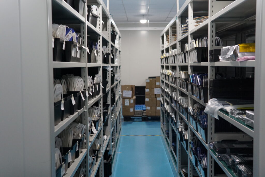
1.Electronic Components Procurement
Purchase all the electronic components required and ensure the quality of each component
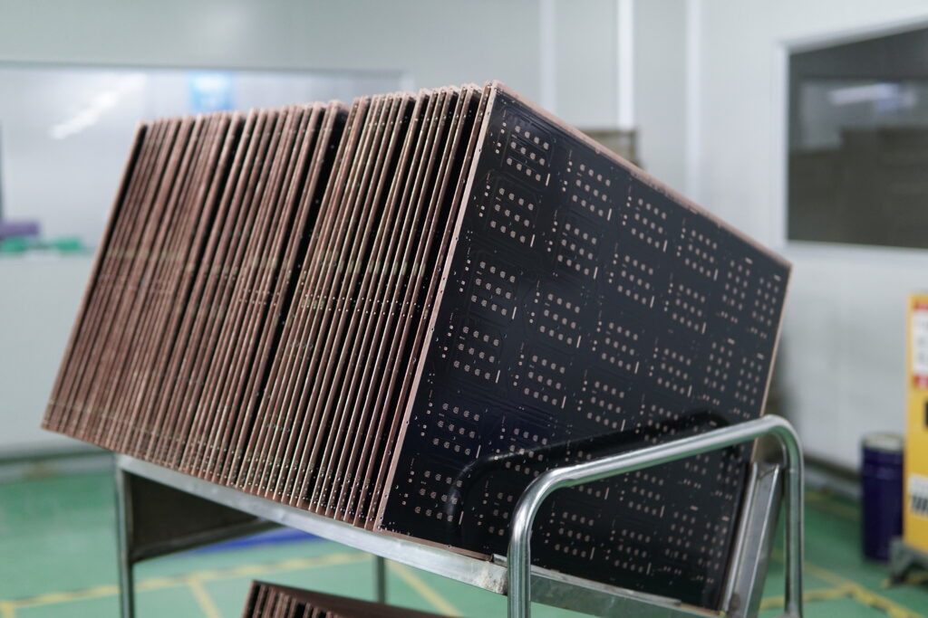
2.PCB production
PCB manufacturing,Make PCBs according to the PCB drawings. Ensure the PCB circuits are complete and the pads are positioned accurately.
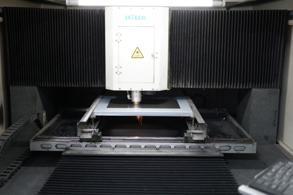
3. Make a steel mesh.
Make a steel mesh file through the PCB assembly file. Usually, stainless steel is used to punch holes on it by laser or electroforming according to the steel mesh file to facilitate subsequent solder paste printing.
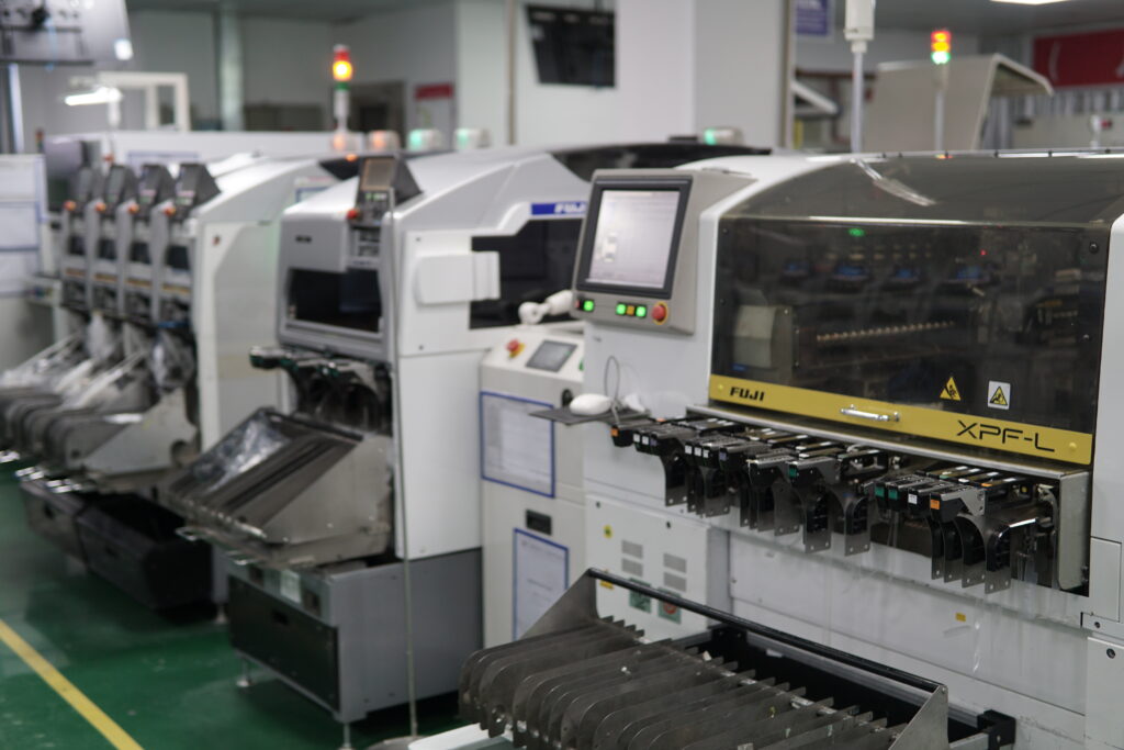
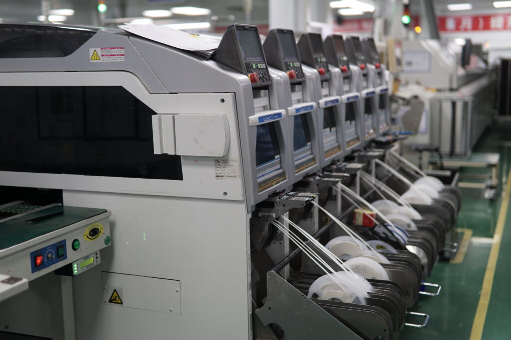
4. SMT machine programming
Professional technicians program the SMT placement machine and feed the PCB into the SMT placement machine. The placement machine picks up the correct components and places each component in the corresponding position accurately according to the pre-programmed program.
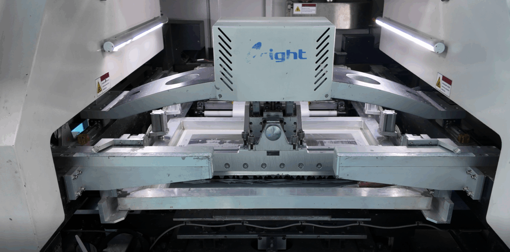
5. Solder paste printing
Solder paste is a mixture of solder resist and tin. The stencils are aligned and stacked on the PCB, and the printer uses a scraper to print the solder paste on the PCB. The thickness of the solder paste on the PCB is determined by the thickness of the stencil and the scraper pressure, so the scraper pressure needs to be controlled.
6. SPI (Solder Paste Inspection).
This is a machine that inspects the solder paste on the PCB board. The laser measures the thickness, area, and flatness of the solder paste to determine whether the components can be soldered well.
7. Inspection before reflow soldering
Check whether the machine has printed the solder paste onto the PCB. If there is a problem with the printing, the PCB will be sent back to the previous process until it is qualified.
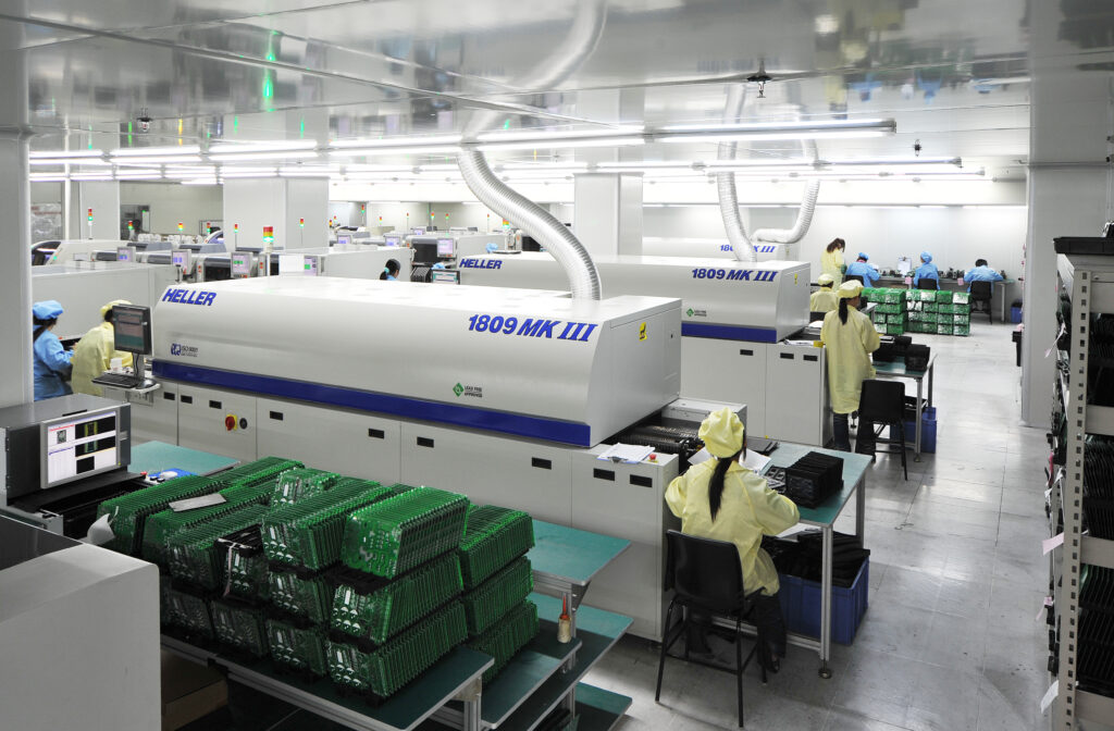
8. Reflow soldering
The solder paste on the pad melts at high temperature, allowing the tin to cover the connection of the components, and then cools and solidifies.
9. AOI (Automated Optical Inspection)
Utilize 3D technology and 3D physical optical imaging to accurately detect and identify possible defects.
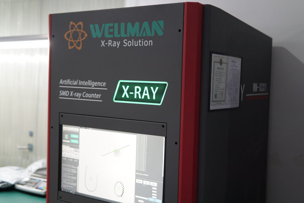
10. X-ray inspection
After assembly, if there are BGA chips on the PCB, the pins of the BGA chip are different from the conventional design. The conventional design has pins distributed around the chip, while the BGA is distributed at the bottom of the chip. Therefore, it is difficult to judge whether the soldering is qualified with the naked eye. Then we will use the penetrating power of X-rays to detect.
11. Cleaning and drying.
During the entire production process, some impurities or oil stains will be generated, which may remain on the surface of the PCB, so they will be cleaned and dried with clean water or chemical solutions.
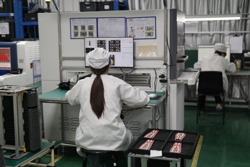
12.SMT QA (Quality Assurance).
We check the PCB again and test the PCB, check the results of SMT assembly, and ensure that the product delivered to the customer is a qualified and high-quality product.
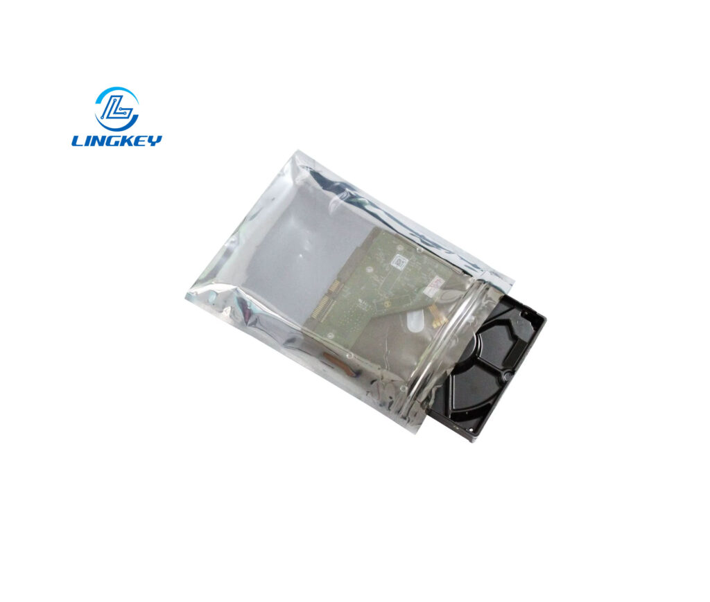
13. Anti-static bag packaging
Anti-static packaging is necessary to prevent static electricity from damaging electronic components.
LingKey is Trustworthy
LingKeypcb is a high-tech enterprise specializing in the research and development and production of customized automation equipment. Founded in 2005, LingKeypcb’s R&D center is located in Huizhou, China. After years of development, LingKeypcb now employs over 400 people, operates a 23,000-square-meter factory, and boasts an annual output exceeding RMB 100 million.
The company boasts a comprehensive SMT production line equipped with high-speed placement machines, fully automatic solder paste printing and inspection equipment, reflow ovens, AOI optical inspection, and X-ray inspection systems, meeting diverse needs from prototype trials to mass production. With its high-precision manufacturing processes, efficient production capacity, and stringent quality control systems, LingKey PCB has earned the trust and long-term partnership of clients across numerous industries, including consumer electronics, automotive electronics, communications equipment, and medical electronics.
