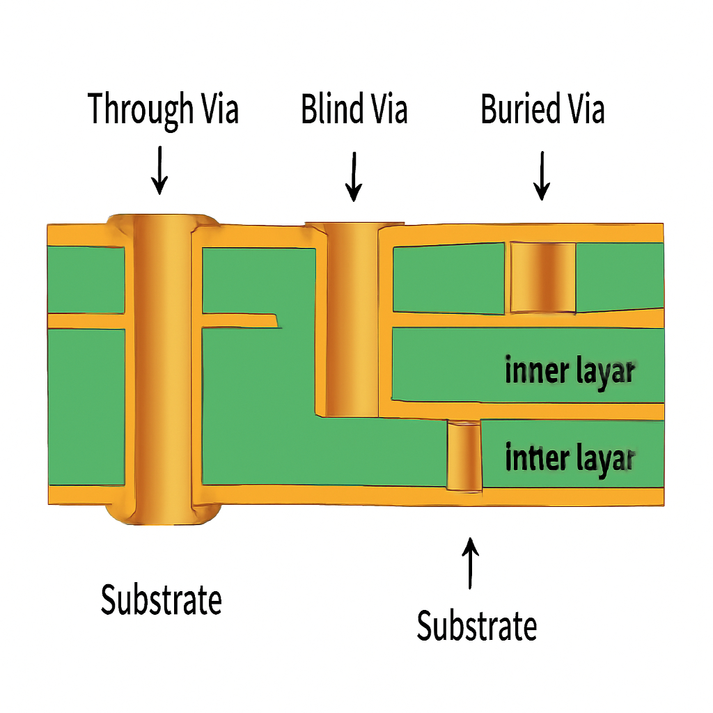
Blind Vias
Blind Vias are special vias used on PCBs (Printed Circuit Boards). They start from the outer layer and connect to the inner layer. These holes do not penetrate the entire circuit. Their function is to connect at least one inner layer to the outer layer. After these holes are pressed together, the other end will not be visible, so they are called blind vias.
Why Use Blind Vias?
As the modern market evolves, electronic products are becoming smaller and more functional, driving the need for higher trace density on circuit boards. Traditional through-holes (THVs) run through the entire board, occupying significant space and limiting trace distribution. Blind vias, on the other hand, connect only the required layers, significantly improving efficiency and space utilization.
Key Features of Blind Vias
1. Space Saving and Increased Routing Density
Because blind vias do not penetrate the entire PCB, they only connect one or more inner layers. This effectively saves internal space, allowing engineers to implement more complex circuit layouts within limited space.
2. Optimize signal transmission performance.
Compared to through-holes, blind vias have shorter paths, which can reduce signal delay and reflection, lower electromagnetic interference, and ensure more complete transmission on the PCB.
3. Supports Lighter Products
Blind vias can reduce PCB thickness and the number of layers, enabling miniaturized and lightweight designs for some electronic products.
4. Improve product reliability.
Blind vias are created using advanced laser drilling and electroplating techniques, making the electrical connection more stable and thus improving product reliability.
Blind Via Fabrication Methods
1. Laser Drilling
A high-energy laser is used to ablate micro blind vias in copper foil and dielectric materials.
2. Mechanical Drilling
Use a high-speed drilling machine to drill holes from the outer layer to the inner layer.
3. Electroplating and Via Filling
After drilling, a conductive layer is formed inside the drilled holes through electroless copper deposition and electroplating, and blind vias are filled with copper.
4. Stacked Via and Staggered Via Structures
Stacked Via: Multiple blind vias are stacked layer by layer, suitable for high-density interconnect structures.
Staggered Via: The blind vias on each layer are staggered, simplifying the manufacturing process.
Flexible adaptation to different stacking designs improves board utilization.
Comparison of three types of vias
Through Hole | Blind Via | Buried Via | |
Number of connection layers | Top to bottom floor | Outer to inner layer | Inner to inner |
Whether it runs through the entire board | Yes | No | No |
Space utilization | Low | High | High |
Manufacturing difficulty | Low | Medium | High |
cost | Low | Medium | High
|
Applicable board type | Standard multilayer board | HDI (High Density Interconnect) board | Advanced multilayer board |
Main Applications | General electronic products | Smart devices, communication equipment | Servers, automotive electronics, industrial control, etc. |
