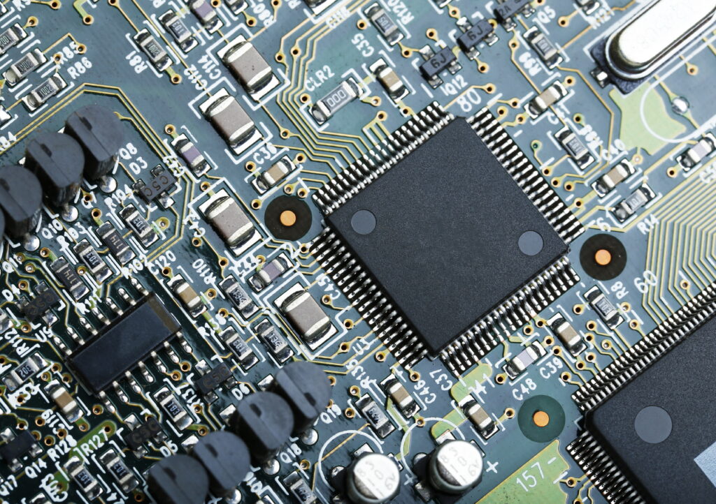
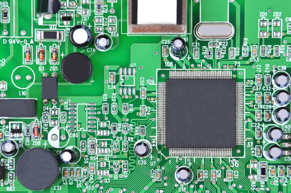
BGA PCB Assembly
BGA is a surface mount packaging technology. Unlike traditional components with pins on the bottom, BGA components have solder balls distributed regularly on their bottoms. During the reflow process, these solder balls melt and then cool, firmly bonding to the PCB pads, creating an electrical and mechanical connection. BGA packaging is ideal for high-density circuits that require high-speed signal transmission and high heat dissipation.
BGA PCB Assembly Process
1. PCB Design and Manufacturing
PCB designs typically use 6 or more layers. To achieve high density, blind and buried vias, and HDI (High Density Interconnect) structures are often incorporated. To ensure secure soldering, PCB design also places high demands on pads, ensuring consistent pad size, a flat surface, and no oxidation.
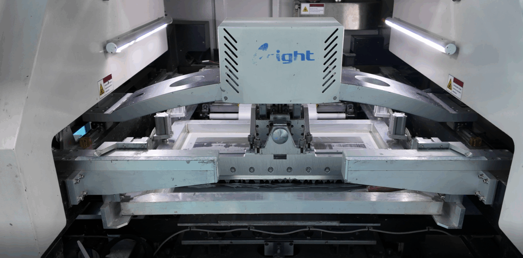
2. Solder Paste Printing
A high-precision laser cuts a stencil, precisely aligning the openings of the stencil with the pads. An automated printer then applies solder paste to the pads, strictly controlling the thickness. The product then passes through an automated solder paste inspection (SPI) to ensure print quality.
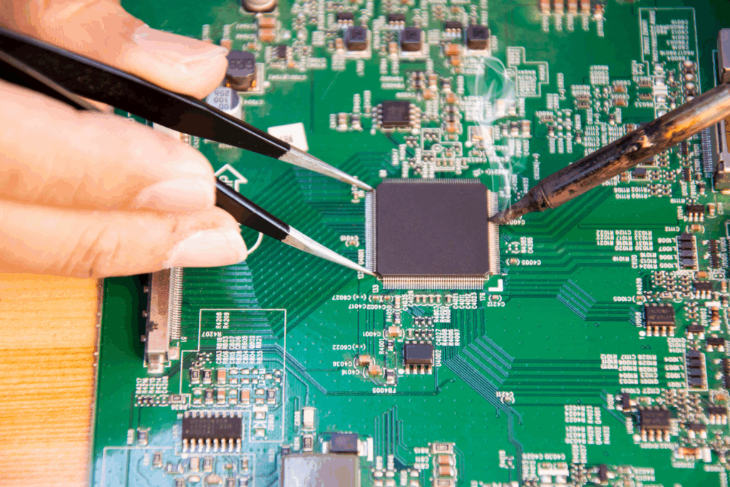
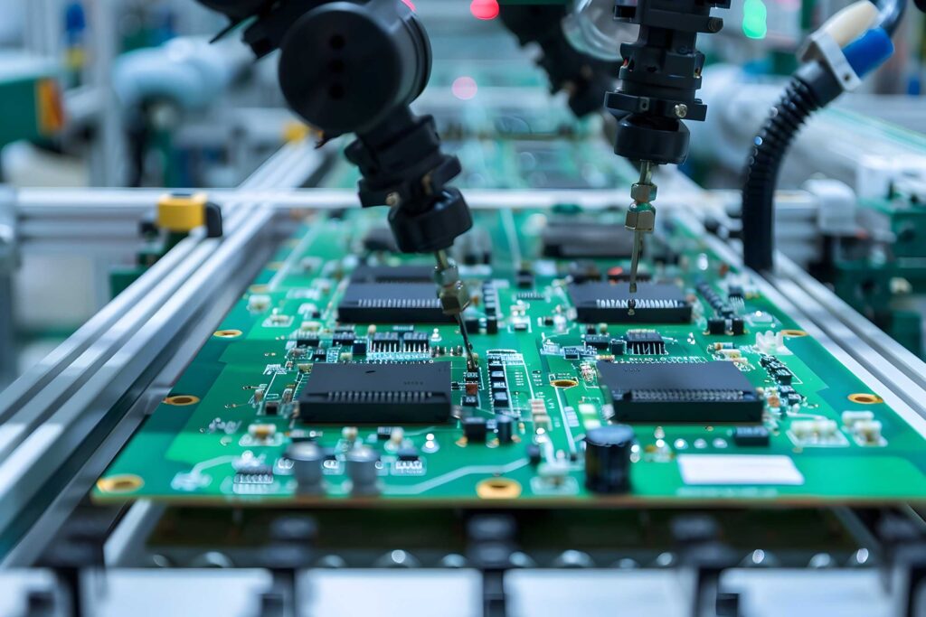
3. BGA component placement
Use an automated placement machine to perform high-speed, high-precision placement of BGA components. The placement machine is equipped with both a flying camera and a fixed camera to provide real-time correction of the placement.
4. Reflow Soldering
The reflow soldering process consists of four stages: preheating, constant temperature, reflow, and cooling. The temperature profile differs from that of conventional PCB reflow soldering. An appropriate temperature profile must be designed according to BGA package specifications, and the heating rate must be strictly controlled to prevent component warping and bending.
5. Inspection
After soldering, the BGA needs to be inspected. Because the BGA solder joints are covered by components, visual inspection is impossible. Therefore, X-rays are used to inspect the solder joints. The BGA also undergoes ICT (In-Circuit Test), FCT (Function Test), and environmental and reliability tests. These tests verify the integrity of the circuit connections and simulate the product’s operating environment to determine if any errors may occur during use.
High-Density Integration
BGA utilizes an array pin design, supporting a higher I/O pin count than traditional packages. Furthermore, the small pitch between pins makes it suitable for high-integration designs and enables more compact product structures.
Excellent heat dissipation
The solder joints are evenly distributed on the bottom of the components, allowing heat from the components to be quickly transferred to the heat dissipation layer inside the PCB.
Excellent Electrical Performance
BGA solder balls connect directly to PCB pads, shortening signal transmission paths and reducing resistance. This effectively increases signal transmission speed.
High reliability
BGA solder joints are spherical in shape, which distributes stress more evenly, reducing the risk of cracking and increasing reliability.
Common Challenges and Solutions for BGA Assembly
Invisible Solder Joints
BGA components’ solder joints are located on the bottom of the package, making them invisible to the naked eye and impossible to detect with traditional AOI. 2D/3D X-ray inspection allows for direct visualization of the solder joint condition and internal structure.
Solder Ball Voids
During the reflow process, if the gas cannot be completely exhausted, voids may form within the solder joint, affecting electrical conductivity and heat dissipation.
Component Warping
BGA packages can warp during heating. During the reflow process, the heating rate and temperature uniformity must be controlled to minimize component warping.
Rework is difficult
Because solder joints are invisible to the naked eye and numerous, rework is more complex than with standard packaging if a problem occurs.
