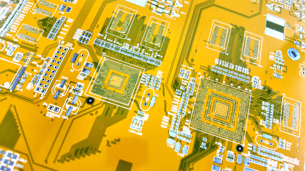
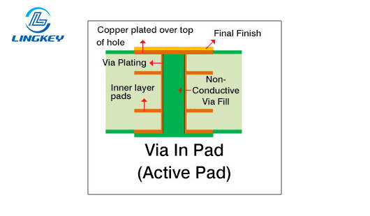
Via-in-Pad
To achieve miniaturization, multifunctionality, and high integration in electronic products, PCB designs must achieve higher routing density. Via-in-pad (VIP) meets this demand. VIP involves placing vias directly beneath surface mount (SMD) pads, rather than routing them around the pads as in traditional designs
Advantages of Via-in-Pad
1.Space Saving
Placing vias directly on pads saves space and eliminates wiring space, making them more suitable for high-density chip packages like BGA and QFN.
2.Improved signal performance
Vias are placed directly on pads, eliminating the need to bypass them. This shortens the signal path, reduces signal delays and interference, and improves signal transmission performance.
3. Improved heat dissipation
Vias in pads can more quickly transfer heat generated by the chip on the pad to the inner layers or back of the PCB, helping to dissipate heat from the component.
4. High-Density Integrated Design
The via-in-pad design allows for a more compact wiring layout, enabling high-density integrated design.
When should you use via-in-pad technology?
Via-in-pad technology offers advantages in the following situations:
1. High-density interconnect (HDI) PCBs
HDI PCBs require higher routing density, necessitating via-in-pad technology to save space.
2. Small Devices
The via-in-pad design is more suitable for devices such as smartphones and smart wearables because it allows for a more compact and efficient design.
3. Improved Electrical Performance
Via-in-pad design reduces inductance and capacitance parasitics by shortening the path, thus enhancing signal integrity.
Design Considerations
- Material Selection: For high-signal or high-frequency applications, materials with stable dielectric constant (DK) and low dielectric loss (DF) should be selected. The thermal conductivity of the material is also important to ensure signal integrity and thermal performance.
- Thermal management: The chip conducts heat through the via design in the pad, which can quickly transfer the heat of the chip to the internal copper layer or the bottom heat dissipation area. Therefore, appropriate thermal vias must be designed to effectively dissipate heat, especially in high-power applications.
Signal integrity: Minimize the number of vias and shorten the via routing length to reduce signal reflections and losses. This improves the electrical performance of the entire board and provides reliable support for high-speed data transmission.
