Single Layer PCB & PCBs: Design, Manufacture, and More
Table of Contents
ToggleIntroduction to Single Layer PCBs
Single layer PCB, or single sided PCB or single sided board, is the most basic type of PCB technology in the electronics industry. It is considered the beginning for many electronics engineers, hobbyists and manufacturers due to the lower cost, ease of assembly, and wide range of applications as a product that has one conductive layer of copperfoil laminated to an insulating substrate. In this all-encompassing design and manufacturing guide, we’ll discuss why single layer boards have stood the test of time despite the proliferation of multi-layer PCBs and complex assemblies.
What Is a Single Layer PCB?
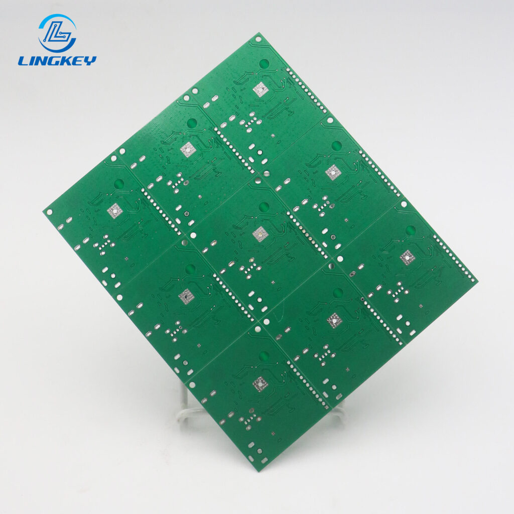
A single layer printed circuit board (also known as single sided pcb board or 1 layer pcb board) is a PCB that has only one layer of copper in which the electrical paths are formed. All components are placed on a single (top) side and the conductive pattern is single sided. Since such a PCB has just one layer of conductive material, the circuit designers must avoid overlapping traces.
There has been progress in multi-layer boards and double-sided technology, but the single layer PCB still has an important purpose – it is applied in many simple consumer, industrial, and lighting electronics products, where complex routing isn’t necessary, but cost-effective, quick, and dependable circuit connectivity is essential.
Basic Structure and Construction of Single Layer PCBs
Key Components of Single Layer PCBs
The board is made from several key materials and features:
- Substrate (Insulating Materials):Commonly FR-4 fiberglass, phenolic resin, or CEM1 for rigidity.
- Copper Foil:Forms the single conductive layer—standard thicknesses are 1 oz or 2 ounces per square foot.
- Solder Mask:Protects copper patterns and defines where solder is permitted during assembly.
- Silkscreen:Printed on the top side to indicate component locations and reference numbers.
Layer | Description |
Silkscreen | Component labels, logos (epoxy ink) |
Solder Mask | Green/colored insulation; blocks undesired solder |
Copper Foil | One conductive layer—traces forming circuits |
Substrate | FR-4 or similar insulating materials |
Single Layer PCB Manufacturing Process
Process of single layer PCB production is enough simple and inexpensive this allowing the quick turnaround time even for custom orders:
- Laminating copper foilonto an insulating substrate.
- Photoresist applicationand exposure to define the circuit pattern.
- Copper etchingto remove unwanted areas, leaving the single conductive
- Drillingcomponent mounting holes.
- Applying solder maskfor protection and electrical performance
- Printing the silkscreenfor assembly guidance.
- Cutting and quality checkswith Automated Optical Inspection (AOI).
This approach allows for low cost and rapid delivery in comparison with multi-layer PCB fabrication.
Types of Single Layer PCBs
Single layer PCBs can be found in many forms, depending on different parameters for use in different applications:
- Rigid Single Layer PCB:Most common, sturdy FR-4 boards for general electronics.
- Flexible Single Layer PCB:Uses polyimide or similar for bendable electronics.
- High-Frequency PCB:Specialized substrate for RF and fast signal switching.
- Aluminum-Backed PCB:Enhanced thermal management for applications like LEDs.
- Rigid-Flex Single-Sided PCB:Merges rigid and flexible for space-constrained designs.
The uses of single layer boards range from consumer products to power modules and to certain medical devices.
Key Features and Unique Advantages of Single Layer PCBs
- Lower cost: Less materials, less complex production and easy assembly.
- Quick turnaround times: Fast design-to-prototype for urgent projects.
- Simple pcba: Straightforward assembly for small- and high-volume runs.
- Good reliabilityin non-complex settings, since trace failures are easy to diagnose.
- Reduced electromagnetic interference: Proper layout can minimize EMI issues despite the absence of multiple ground layers.
- Easier troubleshooting: Visual checking is easier as all traces and pads are on the same side accessible.
Advantages of Single Layer PCBs
- Affordability:The net result is that a number of single sided boards can be made for the same cost as one multi-layer board, thanks to the simplified process.
- Fast prototyping:The simplicity allows for a swift transition from concept to functioning hardware.
- Ease of use:Perfect for education kits, prototyping and applications in which design modifications may be frequent.
- Suitable for a wide range of applications: From remote controls to basic industrial control units.
- Lower risk of failure:No buried vias or complex internal connections.
Disadvantages of Single Layer PCBs
- Limited circuit complexity: Only a single conductivelayer restricts design options.
- Lower component density:Less space for electronic components compared to multi-layer pcbs.
- Less robust electromagnetic interference shielding: May require careful design to avoid noise.
- Thermal management: Designers need to be more aware of the thermal dissipation, especially in power circuits.
- Not ideal for high-performance or compact devices:As consumer expectations elevate, multi-layer boards are frequently required.
Applications of Single Layer PCBs
Single-sided PCBs are found in almost every electronic product and are especially important when the product should be cost efficient as well as simple. A none-exhaustive list:
- Consumer electronics: Calculators, LED lighting, TVs, toys, and home appliances.
- Power modules and supplies: Low-frequency power regulation, adapters, and chargers.
- Industrial control systems: Basic control interfaces, relays, and sensor units.
- Medical electronic devices: Basic monitors, alarms, and dispensers.
- Automotive electronics: Dash displays, switches where complexity is moderate.
- IoT devices: Basic sensors and monitoring units.
- Educational use and prototyping: Beginners’ projects that benefit from easy-to-assemble pcb boards.
Guide to Design: Single Layer PCB Design Considerations
Good PCB design and manufacturing begins with knowing what your needs are. Here’s everything you need to know to design single layer or single sided boards with success:
- Keep traces short and directto improve signal integrity and minimize resistance.
- Group related componentsfor more efficient assembly and maintenance.
- Ensure trace widthmatches current requirements (often measured in ounces per square foot).
- Consider thermal management: Place power-hungry components where heat can dissipate.
- Plan for manufacturability: Avoid features that complicate single layer pcb manufacturing process.
Step-by-Step Design Single Layer PCB
- Define requirements and schematic.
- Select components and footprint—keep in mind space limits of a single-sided board.
- Layout pcb using software, optimizing trace routing and component alignment.
- Run electrical and design rule checksto catch errors.
- Generate Gerber filesand submit to your pcb manufacturer.
- Prototype and test—review for thermal performance, EMI, and physical fitment.
Single Layer vs. Double-Sided vs. Multi-Layer PCBs
As technology and products become more complex, so do the potential PCB stackups.Here is the comparison of single layer PCBs with double-sided and multi-layer boards:
Feature | Single Layer PCB | Double-Sided PCB | Multi-Layer PCB |
Copper Layers | 1 | 2 | 4 or more |
PCB Complexity | Simple | Moderately complex | Highly complex |
Component Density | Low | Medium | High |
Routing Flexibility | Basic | Improved | Extensive |
EMI Performance | Limited (needs careful design) | Enhanced (can add ground planes) | Excellent (multiple planes for EMI shielding) |
Cost | Lower cost | Moderate | Higher |
Electrical Performance | Basic | Good | Advanced |
Turnaround Times | Fast | Moderate | Slow |
Wide Range of Applications | Yes | Yes | Yes |
Single-sided board layouts perform well when reliability, cost, and fast delivery are the dominant factors, while more advanced multi-layer pcb technology is selected for smart devices, high speed data, and space limited consumer electronics.
Cost Factors and Lower Cost Analysis
Selecting a single layer PCB saves a lot of cost for both the development and the mass production.Here’s why:
- Material Savings:With only one copper foil and basic insulating materials, costs are kept minimal.
- Process Efficiency:Fewer steps mean lower cost for both prototyping and full-scale manufacturing.
- Quick Prototyping:Simplified process leads to reduced setup time and lower tooling expenses.
- No Vias or Inter-layer Connections:Removing the complexity of via drilling and plating, the expense and error rates is lowered.
- Greater Yields:Simple structures result in fewer manufacturing defects.
Cost Factor | Single Layer | Double Sided | Multi-Layer |
Copper Foil Used | 1 side | 2 sides | 4–16 layers |
Manufacturing Steps | Fewer (Fast) | Moderate | Most (Slowest) |
Material Cost | Lowest | Medium | Highest |
Turnaround Time | 1–3 days | 3–5 days | 5–10 days |
Frequently Asked Questions About Single Layer PCBs
What is the main difference between single layer, double-sided, and multi-layer PCBs?
Can I upgrade my design from a single-sided to a multi-layer board?
When should I use a single-sided board over multi-layer boards?
How does a single layer PCB handle electromagnetic interference?
What determines the final cost of a single layer PCB?
Why Choose LingKey as Your PCB Manufacturer?
As a top rated pcb supplier, we offer full design and manufacturing services for all types of pcb from single pcb and single-layer pcbs to the most complicated multi-layer pcbs.Here’s why we’re selected by engineers in the electronics industry:
- Cutting-edge PCB technology: Modern facilities for all scales of production and pcba.
- Expert design support: Guidance from schematic through layout and prototyping.
- Comprehensive testing: AOI, electrical, and functional tests ensure reliable delivery.
- Fast turnaround times: From prototype to full run, on-time every time.
- Competitive pricing: Enjoy the benefits of lower costsingle layer PCB manufacturing without compromise.
Conclusion: Is a Single Layer PCB Right for You?
In summary, a single layer PCB is the best option in terms of cost, speed and complexity among the other kinds of PCB. Good for fast prototyping and straightforward designs in consumer electronics, industrial applications and educational projects, as well as for high volume manufacturing. Although single-sided boards have some unique benefits in terms of cost and ease of manufacture, more complex products may call for multi-layer PCB design.
With LingKey’s experienc, your previously single-layer PCB designs can now enjoy quick turnaround, dependable quality, and affordable manufacturing. From prototype through production, LingKey guarantees accuracy in fabrication, thorough testing, and expert support to enable your projects to succeed without sacrificing performance or reliability. From educational kits to industrial controllers to consumer electronics, LingKey provides single layer PCB solutions that address the technical and business requirements of your project in an efficient manner.
")
")


")
")
")


