BGA PCB Assembly

The main advantages of BGA assembly

The advantages of BGA assembly make it play an irreplaceable role in the manufacturing of high-performance electronic equipment.

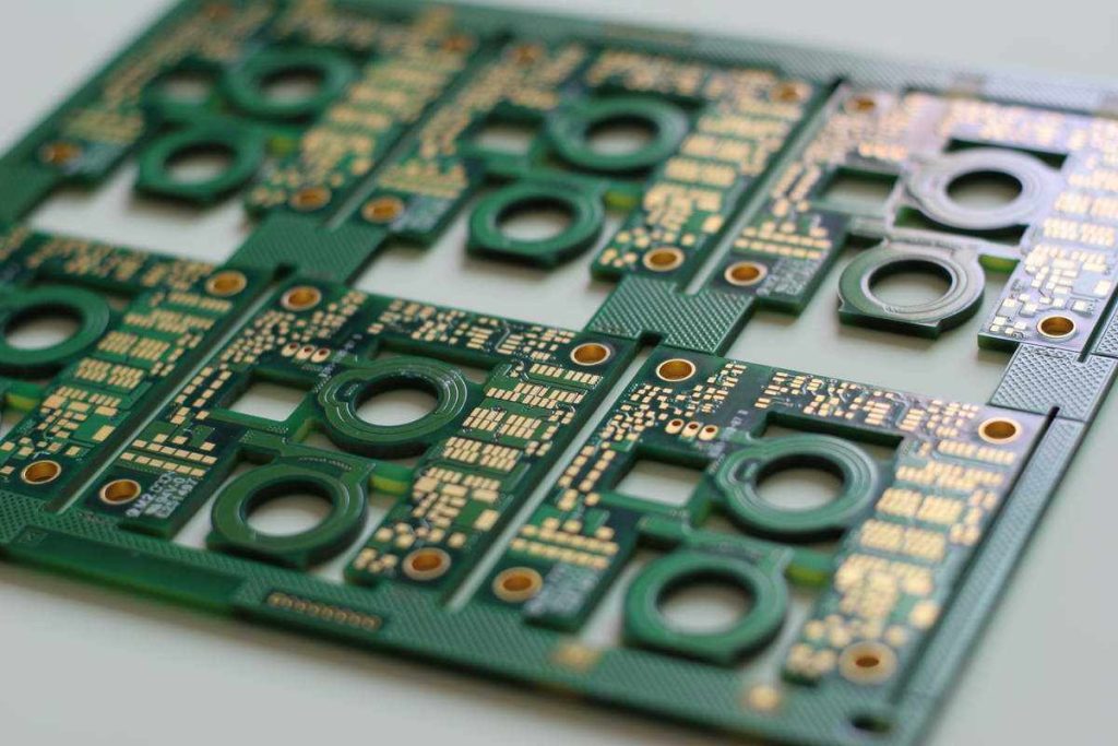
Increased pin density and smaller package size

BGAs can provide more pins in the same or smaller package size because the pins are distributed in a grid across the entire bottom of the chip, rather than just around the edges. This design enables the BGA package to support more I/O ports, which is very suitable for the needs of high-performance multi-functional integrated circuits.

Improved electrical performance

Because the pins of BGA are shorter, the path for electrical signal transmission is shorter, thus reducing signal delay and transmission loss.This is especially important for high-frequency applications because short signal paths can significantly reduce signal attenuation and noise interference, improving the signal integrity of the entire system.

Better thermal management

The design of the BGA package facilitates effective heat conduction.The solder balls help conduct heat generated by the chip into the PCB and further through the PCB to other heat-dissipating components or enclosures. This improvement in heat conduction efficiency is especially important for higher-power equipment, helping to improve its reliability and performance.

Higher reliability

BGA's solder balls provide a larger contact area than traditional pins, which means more stable mechanical and electrical contact at each connection point.In addition, the solder joints of BGA are hidden under the chip and are less likely to be affected by external physical influences, thereby reducing the risk of physical damage.

Simplified PCB layout

Because BGA can carry more pins in a smaller space, PCB designers can use the space on the PCB more efficiently and achieve more compact designs.This not only helps reduce the overall device size but also enables greater flexibility and efficiency in PCB design.

Improved production efficiency

BGA assembly is suitable for standard SMT (surface mount technology) production lines and can be quickly and accurately placed and welded through automated equipment to improve production efficiency. At the same time, the self-positioning feature of BGA makes alignment easier and more accurate during the production process, reducing production errors and improving yield.

Trusted Name for BGA PCB Assembly Solutions

BGA PCB assembly involves attaching components with ball-shaped solder connections arranged in a grid pattern. This design allows for a compact layout, superior electrical performance, and efficient heat dissipation. BGA circuit boards are widely used in devices that demand miniaturization and high performance, such as smartphones, laptops, and medical equipment.
The BGA assembly process ensures better connectivity between the board and its components. It minimizes signal distortion and enhances overall system stability. With technological advancements, BGA PCB assembly has become a preferred choice for industries for innovation and durability in their products.
Features of BGA Circuit Board

BGA circuit boards are known for their unique design and advanced functionality. Below are some of their standout features:

01.

Compact Design

BGAs optimize space by eliminating unnecessary leads, making them ideal for small, high-performance devices.

02.

Thermal Efficiency

The solder balls enhance heat transfer, preventing overheating and improving longevity.

03.

Improved Electrical Performance

Shorter interconnects reduce signal interference, ensuring faster and more reliable communication.

04.

Mechanical Stability

The ball grid structure provides a robust connection, reducing the likelihood of damage during operation.

Why Choose Lingkey for BGA PCB Assembly?

Lingkey offers several distinct advantages that set us apart from competitors:

  1. Cutting-Edge Technology:We use the latest tools and techniques for accurate and efficient BGA assembly.
  2. Custom Solutions:Tailored designs to meet the unique requirements of your project.
  3. Experienced Team:Decades of expertise in PCB manufacturing and assembly.
  4. Strict Quality Control:Comprehensive inspections at every stage to ensure defect-free products.
  5. Competitive Pricing:High-quality solutions at cost-effective rates.
Lingkey's Process and Technical Capabilities

At Lingkey, we specialize in delivering high-quality BGA PCB assembly services tailored to meet your specific needs. Our advanced processes include:

Automated Placement

Ensures precision in positioning BGA components, reducing assembly errors.

X-Ray Inspection

Verifies solder joint integrity, ensuring flawless connections.

Thermal Profiling

Optimizes soldering conditions to maintain component functionality and durability.

Testing & Validation

Rigorous testing ensures your BGA circuit board operates seamlessly under various conditions.

Easy to detect and repair

Although the solder joints of BGA are not visible, modern X-ray inspection technology can be effectively used to detect the quality of solder joints under BGA to ensure the reliability of the connection. In addition, professional equipment and technology can also be used for BGA rework and repair. Although this is more complicated than traditional pin packaging, there are mature technical solutions.

BGA-PCB-Assembly

Common Questions

BGA assembly uses ball-shaped solder connections, offering better heat dissipation, enhanced electrical performance, and a more compact design than traditional leaded assemblies.

Our process includes automated placement, X-ray inspections, and rigorous testing to maintain exceptional quality standards.

Yes, the thermal efficiency and robust connections make it ideal for such conditions.

BGA circuit boards are integral to various industries, including consumer electronics like smartphones and laptops, automotive systems such as ADAS and infotainment, medical devices for diagnostics and monitoring, telecommunications for high-speed networking, and industrial equipment like robotics and automation systems.

The main processes of BGA assembly

01

PCB design and preparation

Before BGA assembly begins, you first need to ensure that the PCB (Printed Circuit Board) design is suitable for the BGA package. This includes designing appropriate pads for the BGA chip, and ensuring that the size, shape, and layout of the pads match the requirements of the BGA package. In addition, proper thermal management and signal integrity measures often need to be designed into the PCB.

02

Printing solder paste

Use a stencil to precisely print the solder paste onto the PCB’s BGA pads. Solder paste usually contains metal powder (usually tin-lead or lead-free tin alloy) and flux. This step is critical to subsequent soldering quality, requiring precise control of the amount and distribution of solder paste.

03

Chip placement

A high-precision placement machine is used to place the BGA chip on the pads coated with solder paste. The placement machine needs to be very precise in aligning the solder balls of the BGA chip with the pads on the PCB, because once placed, small deviations between the solder balls and the pads may cause welding failure.

04

Reflow soldering

Send the PCB board with BGA into the reflow oven for heating. The reflow soldering process includes preheating, thermal activation, reflow, and cooling stages. During this process, the solder paste will melt to form solder joints, which will fix the connection between the BGA chip and the PCB. The temperature profile (temperature versus time) needs to be carefully set to ensure soldering quality and prevent problems such as solder ball collapse or poor soldering.

05

Cleaning

After soldering is completed, the PCB usually needs to be cleaned to remove residual flux and possible soldering residue. This step helps improve the reliability and long-term performance of the circuit.

06

Testing

Since the solder joints of the BGA are located under the chip, the soldering quality cannot be assessed directly through visual inspection. Therefore, X-ray inspection technology is often used to inspect the solder joints under the BGA. X-rays can show the connection between solder balls and pads, helping to identify problems such as air soldering, short circuits, or solder ball bridging.

07

Repair and rework

If the test finds problems, the BGA may need to be repaired or reworked. This typically involves the use of specialized rework stations that use heat and precise control to realign or replace the BGA chips.

08

Functional testing

Finally, functional testing is performed to ensure that the assembled PCB electrically and functionally meets the design specifications. This is the final step to verify the success of the entire assembly process.

Scroll to Top

Contact Us