Burn-in Test for Electronics & PCBs: A Comprehensive Guide
Table of Contents
ToggleIntroduction to Burn-in Testing in Electronics and PCBs
The burn-in testing is now one of the essential elements of the PCB manufacturing process and the electronics reliability guaranteeing. Today, end-users expect electronic devices that work flawlessly, making it increasingly important to guarantee the reliability of PCBs (printed circuit boards). This is especially true for PCB production, where each assembled PCB must not only survive time but a myriad of environmental conditions.
Thermal and electrical stresses on PCBs are chased to extremes during burn-in testing, which allows manufacturers to expose potential weaknesses, confirm design robustness, and rally devices to live in extreme environments well beyond their normal use. The layering of modern pcb design techniques and robust reliability test stages including burn-in significantly improves pcb reliability.
As a professional PCB manufacturer, LingKey also integrates burn-in testing into its reliability program, providing an opportunity for customers to detect early-life failures and promote stable performance in high-risk applications.
What is Burn-in Test in Electronics?
A burn-in test in electronics is a form of active reliability testing that subjects PCBs under test with higher than normal voltages, temperatures, and currents. The process stresses intentionally every feature of the PCB and its components and makes latent defects such as PCB contamination, solder joint problems, and defective components manifest.
The result is that by exposing PCBs to these harsh environments during burn-in testing, the manufacturers can make sure that the PCBs conform to the test parameter for final application, which ensures that the signal integrity of the input and output signals is maintained throughout the application of all load conditions anticipated. This coupling between the PCB design stage and actual field application is critical for mission critical industries that depend on perfect operation.
Importance and Objectives of Burn-in Testing
Why Burn-in Testing Matters
Burn-in testing isn’t just a box to check for reliability—it’s a protection for product quality, brand reputation, and the safety of the customer. It allows producers to:
- Identify potentialand latent failures that typical visual or functional tests might miss.
- Reduce production costsassociated with field service, warranty returns, and recalls by catching faulty PCBs
- Ensure the reliabilityand long-term performance of each unit delivered to the end-user.
- Help meet quality certificationsand industry standards, critical for markets like automotive and medical devices.
- Provide actionable data for continuous improvement in both the design and manufacturing
Fundamental Role in the PCB Manufacturing Process
Burn-in testing helps guarantee that each device will pass through the infant mortality phase, the period during which it is most likely to fail in its lifecycle. The procedure is fully integrated into the pcb production process, especially for those committed to high levels of reliability and quality.
Types of Burn-in Testing
Static Burn-in Testing
Static burn-in testing is a process of applying fixed high voltage and temperature on PCBs or components with power on for a certain period of time. This technique has the advantage to reveal latent defects triggered by long term exposure to stress, like oxidation, contamination of PCB or slow degradation of insulation.
Dynamic Burn-in Testing
Unlike its static counterpart, the dynamic burn-in testing changes electrical inputs and test parameters to simulate the real operating cycles of a product. This can be done by toggling input signals, changing loads or even by running real firmware, which is excellent for identifying intermittent failures, signal integrity problems or subtle design issues.
Accelerated Stress Test
An accelerated stress test imposes more extreme conditions (temperature, voltage/current, cycling rate) to significantly shorten the time to induce failure modes. HTOL (High Temperature Operating Life) and HTGB (High Temperature Gate Bias) among others are widely adopted for semiconductors and other sensitive electronics to reduce the time for bulk screening.
What Burn-in Testing Examines
Burn-in testing is designed to identify potential problem areas at both the component and board levels. Primary targets include:
- Solder Joints: Issues with components soldered onto the PCB, such as cracks, voids, or cold joints.
- PCB Contamination: Flux residue or ionic contaminants that cause corrosion or shorts.
- Thermal and Electrical Stress: Fracturing in traces, copper pads, or vias due to expanding/contracting during cycles.
- Connector Contact Issues and Power Cycling: Troubles with the tightness of the connection during repeated plug/unplugs or power on/off cycles.
- Firmware and Hardware Interactions: Subtle errors only triggered under atypical operating conditions.
Trackable metrics such as MTBF, FIT and DPPM, are important for failure analysis and design and process improvement for design and manufacturing flow.
Burn-in Testing Methods and Metrics
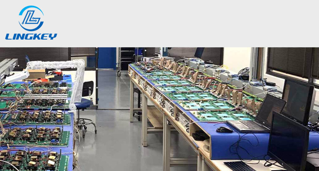
During the burn-in process, the burn-in PCBs are loaded into temperature chambers and exposed to high voltages and thermal cycling. Testers choose test parameters (length, temp, current, voltage) with care to mirror real-world stress. A good-quality test fixture ensures that each assembled PCB is touched consistently and has advanced sensors to measure thermal and electrical performance.
Burn-in test data—including voltages, temperatures, leakage current levels, cycle counts, and failure logs—is collected in real time. Such information is critical for failure analysis, and to document the reliability of the PCBs that are shipped to the regu- lated industries.
Understanding the Burn-in Test Process
Here’s a typical workflow for conducting burn-in:
- Preparation:Each PCB is visually inspected for pcb design flaws, cleaned (to avoid pcb contamination), then loaded into a test fixture designed for electrical and thermal uniformity.
- Execution:The chamber cycles through specified input signals, temperatures, and operating voltages—the test parameters.
- Monitoring:Sensors track all outputs, flagging any deviations from ideal electrical or signal integrity.
- Inspection and Analysis:After the test, engineers inspect the units, performing in-depth failure analysis on any anomalies detected.
- Documentation:All findings are compiled into quality control logs, supporting further improvements in pcb design or manufacturing
Burn-in at Component vs. Board Level
Burn-in testing can be performed at different stages:
- Component-Level Testing:Focus on individual ICs or semiconductors rather than assembled PCB before they are delivered for soldering on the PCB. This advanced testing significantly mitigates the risk of building bad PCBs.
- Board-Level Testing:Tests the entire populated PCB, consisting of all the solder joints, connectors, and the on-board logic, with stress patterns that mimic actual usage. Board-level burn-in is important to detect system integration errors that do not show up at the part level.
Burn-in at two levels significantly improves the reliability of PCBs and testing helps ensure that even the most complex circuits meet design intent.
Common Applications of Burn-in Testing
Defense, Medical, & Automotive Electronics
Applications such as defense electronics, medical devices and automotive systems utilize burn- in as part of their pcb manufacturing process. For example:
- Medical Equipment: Burn-in simulates continuous operation, ensuring life-critical reliability.
- Automotive Electronics: Simulates years of engine bay heat cycles and power surges to ensure that PCBswill last.
- Aerospace Electronics: Verifies that avionics systems withstand vibration, extreme temperatures, and radiation.
These applications exemplify the improvement in product reliability by using burn-in testing in situations in which failure is not an option.
Burn-in Test Equipment and Setup
Burn-in Chambers & Test Fixtures
The effectiveness of burn-in relies on specialized equipment
such as burn-in test chambers and rugged test fixtures. Burn-in chambers provide temperature control (from subzero to over 100°C), humidity control and voltage level control. Automated chamber usage not only improves throughput, but also ensures a consistent stress for every PCB in the process.
Test fixtures are custom engineered to provide a consistent connection to any point on the PCB that requires monitoring. The fixture provides a controlled input signal, power and data lines to the device under test, and the device is fully stressed and measured during the test cycle. Quality fixtures can work with hundreds of boards at a time, which can help keep production costs down in a high volume environment.
Monitoring sensors located inside the fixtures are constantly collecting information about the current, voltage, signal response and thermal hot spots that may point toward a defect or risk of failure. Suppliers commonly use live dashboards to raise alerts and react to anomalies in real time, so that only the most robust assembled PCBs continue down the production line.

Advanced Burn-in Testing Techniques
In order to further the reliability of PCBs the manufacturers usually employ high end techniques like:
Environmental Stress Screening (ESS)
ESS implements burn-in in a more rigorous way by cycling both temperature and humidity, and in some cases vibration, to rapidly weed out candidate early-life failure. This method is critical when circuit boards are deployed in tough environments like military and aerospace applications.
High Temperature Operating Life (HTOL) and Gate Bias (HTGB)
HTOL and HTGB are accelerated stress tests that expose devices to high temperature and voltage for an extended duration. Such processes simulate years of usage in the span of days or weeks, providing a significant increase in confidence of the reliability and quality of the end products.
Thermal and Electrical Cycling
Switching between power-up and power-down states or by raising and lowering the voltage or temperature can stress solder joints, leads on components, and interconnections in ways that reveal latent defects that are not visible under static conditions. Thermal and electrical cycling is commonly employed to augment simple static burn-in testing.
Signal Integrity Monitoring
When the testing is dynamic and at high frequency, sophisticated oscilloscopes and network analyzers are used to monitor the signal integrity on critical traces. This makes sure that such speed-dependent or RF circuits will be robust in actual use, a critical issue especially in telecom and high-frequency markets.
PCB Testing Methods: Comprehensive Guide
Burn-in is included, but it is only one aspect of a more comprehensive PCB quality control and testing that helps ensure PCBs comply with the most rigorous standards.Also included in the pcb fabrication process are:
Test Method | Key Purpose | Typical Use Cases |
In-circuit Testing (ICT) | Detects shorts/opens, verifies components | Mass production, standard PCBs |
Flying Probe Testing | Non-intrusive, flexible for prototyping | Small runs, prototypes, complex boards |
Automated Optical Inspection | Solder, placement, and alignment checks | Soldering and assembly verification |
Solder Paste Inspection | Ensures correct solder application | Surface mount lines |
Boundary Scan | Digital interconnects (JTAG-based) | High-density digital PCBs |
X-ray Inspection | Finds hidden/interior defects (BGAs) | High reliability or complex PCBs |
Functional Testing | Verifies full system under true conditions | Final production testing |
Burn-in & ESS | Long-term and environmental reliability | High reliability /critical use |
Through the integration of these processes such as burn-in testing, the manufacturer can guarantee the reliability of the pcb from the original pcb design stage to the end of the pcb production.
Benefits of Burn-in Testing in PCB Manufacturing
Burn-in testing helps manufacturers in numerous ways:
- Reliability and Quality:Early screening eliminates faulty PCBs before they reach customers.
- Less Field Failure:By reducing early failures and identifying design weaknesses, burn-in increases customer satisfaction and reduces costly service interventions.
- Efficiency:Identifying issues early minimizes waste, rework, and scrap—reducing overall production costs.
- Continuous Improvement:Failure data feeds back into the pcb design and design and manufacturing workflows, prompting better materials, layouts, or assembly processes.
Challenges and Best Practices in Burn-in Testing
While burn-in is vital, it comes with unique challenges, such as:
Challenges:
- Resource Intensity:Burn-in testing can be resource-intensive—requiring energy, time, specialized equipment, and space in the factory.
- Potential Over-stress:If not carefully managed, burn-in could itself cause unrepresentative damage to otherwise good parts.
- Data Overload:Managing and interpreting large volumes of test data (especially in high mix/volume lines) requires robust quality systems and advanced analytics.
Best Practices:
- Define test parametersbased on solid pcb reliability studies and historical failure analysis.
- Design and validate fixtures thoroughly to avoid inducing abnormal stress or harmful mechanical or thermal contact.
- Employ automated monitoring and analysis to handle large datasets, ensuring issues are promptly acted upon.
- Include provisions for feedback from failure analysisto the pcb design phase, enabling continuous process and design improvements.
Latest Trends and Innovations in Burn-in Testing
- Digital Integration:Integration of MES/ERP with burn-in chambers for real-time feedback and traceability.
- Predictive Analytics:AI-driven anomaly detection helps spot subtle trends in test data, enabling proactive design change before costly field failures occur.
- Sustainability:Modern burn-in systems focus on energy efficiency, waste heat recovery, and lean test cycles, supporting green manufacturing goals.
- Design for Testability:DFT principles are now increasingly incorporated in the pcb design stage to make sure the boards are designed for the best possible results when tested all the way—saving resources, and providing better coverage.
FAQ – Burn-in Test in Electronics and PCBs
How do you select the best burn-in test parameters for a new PCB design?
Can burn-in testing improve signal integrity?
How does failure analysis after burn-in inform future PCB design?
Should all PCBs undergo burn-in?
Conclusion – Ensuring Quality & Reliability with Burn-in Testing
Including burn-in testing in your electronics and PCB production process significantly improves the dependability of PCBs that is so important in today’s high-end markets. PCBs are exposed to high levels of stress in a controlled environment so that manufacturers can detect latent defects that would otherwise be detected only in the field.
Through the synergy of disciplined PCB design, controlled manufacturing processes and structured burn-in testing LingKey enables its customers to deliver electronics that meets tight reliability and quality expectations. From prototyping to volume production, LingKey uses burn-in testing as a component of an overall quality assurance system to promote enduring performance in high-reliability applications.
")
")


")
")
")


