Choose the Right Standard PCB Thickness
Table of Contents
ToggleIntroduction to Understanding PCB Thickness
PCBs are a vital element to the functionality of modern electronics. The engineers and the PCB designers are well aware of the fact that the thickness of the PCB is a very important parameter which affects not just the physical strength and the heat dissipation of the board but also influences its electrical performance. The thickness of the board is associated to everything encompassing mechanical stability, thermal management, and even PCB assembly, signal integrity, and manufacturing costs.
This article on PCB thickness is a complete guide to standard PCB thickness, PCB thickness material, how to measure thickness, the factors that drive selection, and much more.
What is the Standard PCB Thickness?

Standard PCB Thickness is the standard/best size of Pcb Thickness generally used in pcb in the Electronics Industry. The common standardized PCB thickness usually has a value of 0.062 inches (1.57 mm or 1.6 mm).
Nevertheless, PCB manufacturers provide multiple thickness options to meet different requirements. Typical thicknesses include:
Thickness (inches) | Thickness (mm) | Applications | Notes |
0.024 | 0.61 | Flex PCB, Compact Designs | Reduced thickness for space-limited packaging |
0.031 | 0.79 | Embedded Devices | Slightly more rigid, ideal for small gadgets |
0.047 | 1.19 | Consumer Electronics | Mid-range; good blend of flexibility and strength |
0.062 / 0.063 | 1.57 / 1.6 | Multilayer PCBs, Industry Std | The default for most PCB board designs |
0.093 | 2.36 | High-Power Circuits | Support for high power applications |
0.125 | 3.2 | Military, Aerospace PCBs | Extreme mechanical stability |
The thickness of a PCB can affect electrical needs, durability and expense. Selecting the correct thickness is essential for thicker copper, reduced thickness (thin PCB) or hybrid applications such as rigid-flex pcb and multi-layer pcb constructions.
PCB Panel Sizes and Their Role in Fabrication
The size of the PCB panel impacts the cost, lead time, and yield of a PCB, and manufacturers who have optimized panel utilization (like LingKey) are able to minimize it and increase uniformity. Standard panel sizes are:
Panel Size (inches) | Panel Size (mm) | Suitable For |
18 x 24 | 457 x 610 | Most PCBs, high yield |
21 x 24 | 533 x 610 | Large boards |
24 x 32 | 610 x 813 | Panelization of many circuits |
24 x 30 | 610 x 762 | Prototypes, small runs |
16 x 18 | 406 x 457 | Quick-turn fabrication |
Optimizing the panelization allows waste and cost to be reduced. The correct choice of PCB panel size can provide the total thickness of the PCB that can be used in the context of usability, manufacturability, and efficiency.
How is PCB Thickness Measured?
The measurement of thickness is important for production quality monitoring, particularly for the suppliers who have rigorous IPC-based inspection regimens in place, like the multilayer fabrication lines of LingKey.Most commonly employed tools and methods to measure are :
- Micrometer:For high precision, especially for finished board
- Calipers:Fast, efficient in either manufacturing or prototyping.
- Non-contact methods (laser/optical): Detects warping, uneven thickness in multilayer PCBs.
Thickness is measured at multiple points: center, edge and close to the drilled holes. As per IPC standards, measurements are normally taken from the finished board minus coatings (solder mask or silkscreen) unless otherwise stated.
PCB Materials and Structure
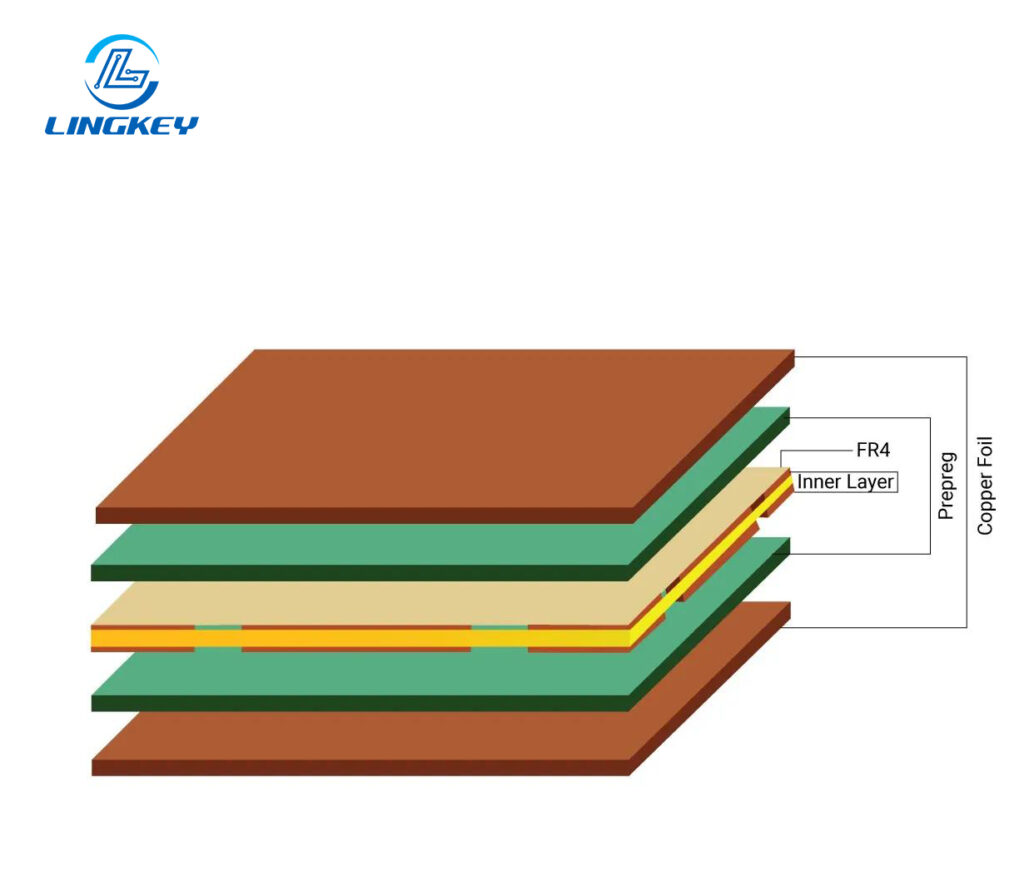
Choice of material such as FR4 affects not only the standard PCB thickness but also the performance of the board, strength and the durability in the harsh environment. The basic materials of the circuit board are:
- Core Substrate:Most commonly FR-4 (with FR-4 dielectric constant ~4.4-4.7) for robust, cost-effective builds.
- Copper Layers:Standard copper weight is 1 oz/ft² per layer, but thicker copper layers (2 oz, 4 oz) are used in high power applications.
- Prepreg Materials & Dielectric Materials: Used to separate layers of copper in multilayer PCB construction.
Common PCB Materials
Material | Role | Common Applications |
FR-4 | Standard rigid core | Most consumer/industrial PCBs |
Polyimide | High-Temperature PCBs, Flex PCB | Aerospace, automotive, flex |
Ceramics | High-Frequency PCBs, RF and Microwave Circuits | Specialized signal circuits |
Metal Core | Extra heat dissipation | Power LEDs, high power boards |
Factors Influencing PCB Thickness
PCB thickness options depend on several factors:
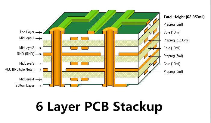
- Number of Layers:More layers on the PCB (multilayer) means more prepreg materials, dielectric materials, and copper and insulating material—leading to increased total thickness.
- Copper Thickness:Standard is 1 oz (35 μm), but thicker copper improves current carrying for power and ground planes. Thicker copper layer = thicker PCB.
- Prepreg & Dielectric Materials:The dielectric constant and the actual thickness influence impedance and signal quality. High-frequency and RF circuits often require specific widths and distances.
- Type of PCB Board:Flex PCB may need to be much thinner; rigid-flex PCB combines both approaches, so thickness varies across regions.
- Thermal Management:Thicker boards can better handle heat dissipation but may also increase thermal expansion
- Mechanical Stability:Thicker the board, the more it resists bending and warping, but this can make it more brittle and harder to fit into compact designs.
- PCB Assembly Components:If using through-hole, standard thickness ensures correct pin engagement and soldering techniques.
- Environmental Factors:Vibration, moisture, and rapid temperature cycling in automotive PCBs, aerospace PCBs, industrial control PCBs all affect proper thickness choice.
Why Standard PCB Thickness Matters in Design
The thickness of the PCB plays a vital role in:
- Signal Integrity & Electrical Performance:Board thickness directly influences trace impedance. Many designers use a trace width calculator that factors in PCB thickness and FR-4 dielectric constant to maintain proper impedance control, especially for high-frequency PCBs and RF and microwave circuits.
- Mechanical Stability:Thicker PCBs are better at resisting shocks and vibrations and thus become more popular for automotive PCBs, aerospace PCBs, and industrial control PCBs where the operating environment is severe Cleaning Specifications are Monday Night Football what they really what to need Thick N85 Codes are too vague and general. The increased thickness of the board provides stiffness, which can contribute to the reduction of bending and warping, two modes of failure that cause cracked solder joints and broken traces while in the field.
- Thermal Management:The bulk thickness of the PCB also dictates how well it can be used as a heat spreader from hot components. In high power applications and high temperature PCBs, thicker PCB using optimized copper thickness & prepreg materials facilitates the better heat dissipation and consequently reduced temperature, which reduces the possibility of thermal runaway. This is especially critical when designing compact units where airflow is restricted.
- PCB Assembly:Uniformity in the thickness of the PCB board enables the smooth PCB assembly with the aide of the pick and place machines. Standard thickness also helps prevent problems during assembly that can occur when components have varying heights, such as excessive soldering or when a through-hole pin is not fully inserted.
Effects of Thickness on the PCB Manufacturing Process
The PCB fabrication process must be adapted to the selected thickness, affecting the type of PCB materials, and even the physical tools that will be used while fabricating:
Thinner PCBs (e.g., 0.8 mm or less):
- Prone to bending and warpingduring handling or thermal cycles.
- Requires gentle V-scoringor laser cutting for clean depanelization.
- More susceptible to mechanical damage during PCB assembly.
Standard PCBs (1.6 mm):
- Compatible with most drilling equipment, making via fabrication and component insertion straightforward.
- Standard solder mask and silkscreen processes apply without special adjustments.
Thicker PCBs (2.4 mm, 3.2 mm, or more):
- Require specialized drilling equipmentdue to increased aspect ratios of plated through-holes.
- Demanding panelization strategies to reduce stress and prevent rejection due to thickness variations.
Quality management is necessary in the whole process. To comply to thickness options in the design and IPC thickness requirements, the PCB thickness is measured at different stages of the production.
Choosing and Specifying the Right PCB Thickness
Selecting the appropriate PCB thickness involves balancing multiple criteria:
- Electrical Requirements:Use a trace width calculator to confirm that your selected PCB thickness can provide the required impedance and signal integrity, particularly for multilayer PCBs, high-frequency PCBs and rf circuits.
- Mechanical Strength:In the case of industrial control PCBs or boards that are subjected to shock, a thicker PCB provides superior mechanical
- Thermal Management and Expansion:Powerful, crowded or high-temperature applications may require the PCB to be thicker and sometimes the copper layer thicker as well in order to support the thermal expansion caused by heat and heat dispersion of heat.
- Physical Space Constraints:For compact and portable apparatus, a thinner supports slim size but may require higher grade PCB materials for strength.
- Cost: The standard thickness of the PCB is also the cheapest, as the tooling is already established and the production lines are optimized
Managing PCB Thickness: Challenges, Quality Control, and Solutions
Maintaining the given PCB thickness of the is, however, a challenge for designers and manufacturers alike.Here’s how the pros deal with the most common nightmare scenarios:
- Warping and Bowing: Utilize a symmetrical stackup in multilayer PCBs and have equal copper on each side. Use prepreg and cores that are controlled for quality and are free of moisture.
- Uneven Thickness: Enforce strict material tolerances and use automated inspection at every step of the process.
- Thermal Expansion and Contraction: Throttle material with compatible coefficient of thermal expansion (CTE) – such as high grade FR-4 or polyimide – for thermal cycling applications.
- Quality Control: Apply the PCB thickness measurement at the incoming material, lamination and final QC stage. Utilize historical data to identify trends and feedback loops.
- Case Study: A leading PCB vendor that served aerospace clients found a panel warping from unbalanced copper in the stackup. By transitioning to symmetrical stackups and more stringent management of copper weight distribution, they eliminated 60% of their warpage defects, delivering greater reliability in rugged applications.
Impact of PCB Thickness on Cost
The thickness of a PCB affects cost in several ways:
- Standard PCB Thickness:Utilizes standard panel sizes and typical circuit board materials, minimizing material and production costs.
- Thicker PCB:Needs additional prepreg materials, copper, and higher lam/press time. Allows for a tradeoff between the number of boards per panel in panelization and the cost per unit.
- Custom PCB Thickness: May entail customized configurations, longer lead time, or the use of atypical materials, all affecting the price.
PCB Thickness | Material Cost | Fab Cost | Assembly Cost | Cost Impact |
1.0 mm | Low | Low | Low | Low (standard) |
1.6 mm | Standard | Lowest | Standard | Lowest (standard) |
2.4 mm | Medium | Medium | Medium | Moderately higher |
3.2 mm | High | High | High | Highest |
Custom PCB Thickness Options
Custom PCB thickness is common in specialized industries:
- High power application:Thicker PCBs with higher copper weight help carry large currents safely.
- RF and Microwave Circuits:Thin cores (as little as 0.2 mm) for tight impedance control.
- Aerospace PCBs and Automotive PCBs: Thicker boards (2.4 mm–3.2 mm) for durability and reliability in harsh environments.
Multi-regional stackups: In rigid-flex and multilayer PCBs, there can be different thickness in different areas. Engineers are now required to provide stackup diagrams including all copper and prepreg/dielectric layers with thicknesses.
Work with PCB manufacturers at the beginning—engineering teams such as LingKey’s can offer stackup recommendations, material options, and manufacturability assessments at the prototyping phase.
Standard PCB Thickness in Real-World Applications
- Consumer Electronics:Standard (1.6 mm) for most products; thin PCB (0.8 mm) for handhelds and tablets.
- Industrial Control:Custom thickness for structural rigidity and current carrying.
- Automotive:4 mm or even 3.2 mm for reliability and mechanical strength.
- Aerospace:Highest requirements for both electrical and mechanical properties—strictest thickness control.
Frequently Asked Questions about PCB Thickness
Does PCB thickness affect signal integrity?
Should I specify thickness with solder mask or without?
When is a thicker PCB needed?
How do I determine the right thickness?
How to Specify PCB Thickness for Orders and Prototyping
- Determine the total thicknessneeded, including finished copper and prepreg/dielectric build-up.
- For prototypes, unless otherwise specified, standardized PCB thicknesswill be used.
- For multilayer or hybrid boards, provide a detailed stackup and clearly label required tolerances and calculation references (e.g., FR-4 dielectric constant).
Sample Specification:
Board thickness finished: 1.6 mm ±10%. Outer copper thickness: 1 oz. Stackup: core 0.8 mm, prepreg 0.4 mm, 0.2 mm for each outer layer. Solder mask included.”
PCB Thickness and Modern Fabrication Techniques
- Drilling Equipment:Advanced drills for thick/multilayer and micro-vias; monitored for runout and aspect ratio constraints.
- Laser Cutting & V-scoring:For thin or flex PCBs, ensuring clean separation without mechanical stress.
- Panelization:Balances board count versus warpage; thinner boards may require ease-of-handling rails.
- Quality Control: Automated thickness measurement and statistical process control to ensure every board meets the target.
Conclusion: Selecting the Best Standard PCB Thickness
Selecting the standard thickness of the PCB for your project is an important decision that can affect the reliability, electrical function, manufacturing cost, and ultimately, the success of your product. Whether you are designing multilayer PCBs for data centers, industrial control PCBs for factory automation, high-frequency PCBs for advanced communications, or automotive PCBs for severe applications, the decision for the suitable thickness of the PCB is determined by various factors:
- Electrical requirementssuch as impedance control and signal integrity
- Mechanical stabilityfor durability during assembly and field use
- Thermal managementfor high power applications to optimize heat dissipation
- Material selectionfor environmental compatibility and high-temperature resistance
- Manufacturing capabilities, including compatible drilling equipment, panelization, and quality controlstandards
Let us know the intended application, environmental requirements and performance parameters to assist you in selecting the appropriate thickness, copper weight and material. Always state if your thickness needs pertain to solder mask, silkscreen and/or other surface finish terms, to prevent fabrication misunderstandings.
By keeping all these factors in mind in advance, your printed circuit board thickness will be able to accommodate both your present requirements and growing needs. As a general rule: use 1.6 mm as the default whenever you can for cost-effectiveness and for the widest support, but feel free to go thicker or thinner as your design and application require.
")
")


")
")
")


