Comprehensive Guide to PCB Test & PCB Testing Methods in PCB Manufacturing
Table of Contents
ToggleIntroduction to PCB Testing

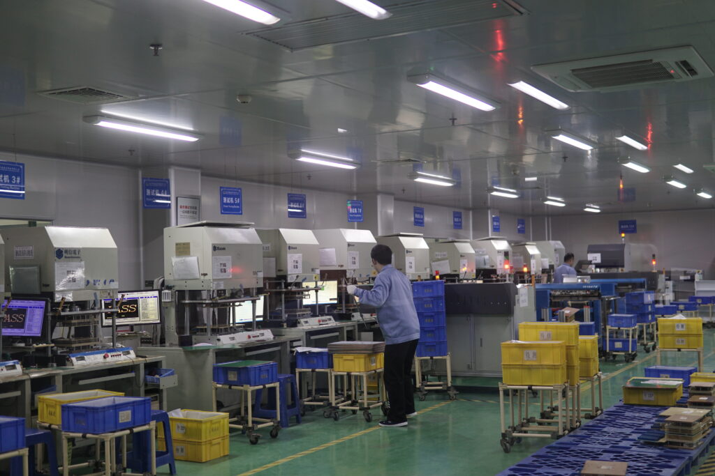
PCB Testing or Circuit Board Testing is a series of critical tests that must be performed to verify the functionality, reliability, and safety of all PCBs (Printed Circuit Board) and PCBAs (Printed Circuit Board Assembly). Due to more complex PCB designs and higher performance and safety requirements with the industry growing, testing of the PCB is a mandatory procedure in electronics manufacturing nowadays.
Techniques for PCB testing are employed in all stages of the development lifecycle – from design and prototype assembly, to the production volume ramp, and as thorough, final tests prior to customer delivery.
From visual inspection to complex electrical connectivity testing, testing allows for potential problems that would lead to the production of bad pcbs, shorts, and product recalls, to be detected and corrected early.
Why PCB Testing is Crucial
Testing is an essential aspect of the pcb production process. ESD related defects are easy to miss without complete verification by different testing methods and tools, resulting in incomplete solder joints, misaligned components, etc.thermal links also can be finished products.
Importance of PCB Testing includes:
- Defect Detection:Identifies flaws in solder connections, copper layers, and substrate integrity.
- Ensuring Product Quality:Verifies that electrical connections and individual components meet design intent.
- Cost Efficiency:Finds issues early, preventing costly field failures and repairs.
- Meeting Quality Standards:Guarantees compliance with IPC, ISO, UL, and RoHS standards.
- Improved Reliability:Effective PCB testing methods directly raise the reliability and safety of the end product.
- Supports Advanced PCB Manufacturing:Adapts to increasing complexity of PCB designs, especially with high-density PCBs and embedded systems.
PCB Testing in Manufacturing
PCB testing is essential from prototyping through high volume production. Test strategies are chosen based on the complexity of the PCB, the production volume and the application.
PCB Testing Involves These Stages:
- Design & Prototype Verification:Testing new PCB designs to verify layout accuracy and ease of assembly.
- In-Process Inspection:Checking the surface of the PCB and copper layer integrity during fabrication.
- Assembly Process Testing:Using circuit board inspection techniques during PCBA for solder mask verification, component alignment, and solderability testing.
- Final Electrical Test:Ensuring all electrical connections on the PCB meet design standards.
Overview of PCB and PCBA Capabilities
Production Capabilities Include:
- Advanced PCB Stackups:Supporting high-density PCBs, heavy copper for power electronics, and thermal shock resistance.
- Quick Turn PCB & Prototype Assembly:Rapid turnaround for new design verification and effective PCB testing at early development stages.
- PCBA (Printed Circuit Board Assembly):Comprehensive PCB assembly and testing services ensure every circuit card assembly meets quality standards.
- Surface Mount Simulation:Allows for accurate component soldering, minimizing manufacturing defects.
- Inspection Methods:Range from human visual inspection to X-ray imaging, micro-sectioning analysis, and automated optical inspection.
Types of PCB Testing Methods
Here are the most effective PCB testing methods and where they fit in the testing process:
Visual Inspection
Checks for obvious manufacturing defects, such as incorrect solder mask application, poor component alignment, and substrate damage. Both manual and camera-based visual inspection methods are common.
Automated Optical Inspection (AOI)

AOI employs a camera or many cameras and uses advanced image processing algorithms to identify defects rapidly such as component misplacement, polarity errors, and solder joint defects on the surface of the PCB. AOI is necessary for mass production.
In-Circuit Testing (ICT)
ICT testing (also known as Electrical Test) uses a bed-of-nails fixture or flying probes to individually check each electrical connection, solder joint, and component on the board. Great for fault isolation and mass production.
Flying Probe Testing
Flying probe testing is a flexible and fixtureless technique for low and medium production volumes, perfect for prototype verification. Automated probes test for opens, shorts, and correct values.
Functional Testing (FCT)
This suite of functional testing methods subjects the PCB or PCBA to real-world operation and stress, confirming the entire assembly works as specified. Every design should pass a thorough PCB functional test before release.
Burn-In Testing
The burn-in test is a rigorouse simulation environmental test to screen out early life failures. Stressing with voltage, current, and temperature over time allows weak boards to be weeded out before they go out the door—critical for high-reliability industries.
X-ray Inspection (AXI)
AXI (Automated X-ray Inspection) visualizes hidden solder joints, copper layers, and BGA connections, revealing internal faults invisible to cameras.
Boundary-Scan Method (JTAG)
This electronic test technique checks connections and logic in complex or high-density PCBs using integrated test logic. Boundary-scan is key for boards where physical access is limited.
Additional Board Testing Methods
- Solderability Test(Wetting Balance Analysis)
- Contamination Testing
- Thermal Shock Testing
- GM/LTS Testing(Global/Local Track Short)
- Micro-Sectioning Analysis
- Time-Domain Reflectometry (TDR)for signal integrity
Step-by-Step PCB Testing Procedures
How to Test a PCB Board:
- Visual Inspection:Assesses solder mask, component placement, copper layer integrity, and obvious defects.
- Continuity Testing:Confirms proper electrical connection between test points on the PCB, checking for open circuits or shorts.
- Automated Optical Inspection (AOI):Detects misalignments and solder bridges during the assembly process.
- Electrical Performance Test:Uses in-circuit testing (ICT) and probe techniques to check all critical points.
- Functional Testing:Simulates real operating scenarios, confirming the PCB functions as specified.
- Burn-In / Environmental Testing:Subjects PCB to temperature extremes, humidity, and voltage for reliability checks.
- X-ray Imaging and Micro-Sectioning:Used for final quality control and to resolve complex faults or design for testing analysis.
Comparing Popular PCB Testing Methods
Here’s a comprehensive comparison of common PCB testing methods:
Testing Method | Best For | Type of Test | Pros | Cons |
Visual Inspection | All PCBs | Manual, Automated | Simple, low-cost, instant feedback | Limited for small defects / hidden joints |
AOI (Automated Optical) | High-volume, fine-pitch SMT | Automated | Fast, accurate, repeatable | Surface-only, can’t “see” inside PCB |
In-Circuit Testing (ICT) | Mass production | Automated fixture | Comprehensive electrical test | Costly fixtures, not flexible for new designs |
Flying Probe Testing | Prototypes, low-volume | Automated | Flexible, no fixture needed | Slower than ICT for large batches |
Functional Testing | All volumes, system validation | Automated/manual | Real-use performance validation | Needs test setup customization |
Burn-In Testing | Critical/Harsh environments | Environmental | Filters out weak units, reliability proof | Not cost-effective for all products |
X-ray Inspection (AXI) | BGAs/multilayer, HDI | Imaging | Finds hidden/internal defects | Expensive, slow, needs operator expertise |
Boundary-Scan/JTAG (JTAG) | Dense PCBs/limited access | Electronic Test | Great for high-density/complex circuits | Requires compatible design, special setup |
GM/LTS Testing | Complex & multilayer PCBs | Automated | Advanced fault isolation for shorts/opens | Specialized, more used in advanced manufacturing |
Solderability Testing | All PCBs, reliability | Physical/Chemical | Ensures strong solder joints/wettin | May need destructive sample, not for all boards |
Environmental Simulation Tests | Harsh or regulated industries | Environmental | Validates real-world reliability (thermal shock, humidity, vibration) | Can be time/resource intensive |
Micro-Sectioning Analysis | Failure analysis/quality audits | Destructive | Reveals internal/fatal flaws for in-depth analysis | Sample destructive, used for audit not QC routine |
TDR (Time-Domain Reflectometry) | High-speed, signal integrity needs | Electrical Analysis | Precise impedance/signal path verification | Specialized tools & setup required |
Why choose LingKey's PCB testing technology?
LingKey’s PCB testing technology has the following advantages:
- PCB Complexity:High-density, multilayer boards and embedded systems often require AXI, TDR, boundary-scan, and environmental testing.
- Production Volume:AOI and ICT dominate high-volume production, while flying probe and visual inspection suit prototypes or low-volume runs.
- Board Functionality:Functional testing confirms real-world operation—essential for PCBA and finished products.
- Regulatory and Quality Standards:Classes of PCBs (IPC, ISO) may require specific tests, wetting balance analysis, or comprehensive environmental tests.
- Design For Testing (DFT):Including accessible test points on the PCB, and ensuring you can hold the PCB in place during testing, dramatically increases test effectiveness and reliability.
Testing Integration in the PCB Manufacturing Process
Incorporation of tests at every level of the PCB production process is crucial for the early detection of defects and to ease the burden of final inspection and rework. PCB testing involves:
- Pre-Fabrication Testing:Validation of Gerber files and design rules before production.
- Bare Board Electrical Testing:Ensuring all netlists are connected and isolated as designed—critical in high-density PCBs.
- Assembly Testing:AOI, ICT, flying probe, and solderability testing during and after the assembly process for component integrity and solder joints.
- Post-Assembly Simulation:Environmental simulation tests (burn-in, thermal shock) and in-system functional testing to confirm long-term PCB reliability.
- Final Inspection Reports & Documentation:Comprehensive result logging, providing manufacturers and customers with clear, traceable data for every test performed.
Detecting and Repairing PCB Defects

Manufacturing defects and component integrity issues can occur at every manufacturing stage. Thorough defect detection employs:
- Visual Inspectionfor surface flaws and component misalignment.
- AOI and AXIfor solder joint quality and hidden voids.
- Electrical Connection Testing(ICT and flying probe) for open/short circuits.
- Burn-in and Environmental Simulationfor reliability under harsh environments.
- Solderability and contamination testingfor ensuring the quality of solder connections.
Cost of Repairs: Early diagnosis translates to reduced costs. Finding a short or bad solder joint in prototyping is way cheaper than doing a field fix after shipping products.
Quality Standards, Compliance, and Test Reporting
Each testing method must produce clear, actionable inspection reports, supporting quality control and regulatory sign-off. Key elements:
- Meets Industry Standards:IPC, UL, ISO for product safety and reliability.
- Inspection Report:Documents every electrical test, failure mode, and corrective action.
- Traceability:All PCBs and PCBA batches are serialized for tracking test results and defect history.
- Continuous Improvement:Data from test reports inform future PCB design improvements and assembly process optimizations.
PCB Testing FAQs
Why is PCB testing crucial?
What testing methods are used for complex PCB designs?
How do I select the right PCB testing methods?
What equipment is used for PCB testing
Can testing software automate PCB testing?
Conclusion: The Benefits of Effective PCB Testing
Efficient methods for testing the PCB are the key to a stable product development and the assurance that the printed circuit board and circuit card assembly is ready to go out in the field. Whether you’re evaluating new designs for PCBs, confirming your PCBA’s reliability, or achieving the highest quality for the most demanding environments, it’s important to select the right test method. The advantages of pcb testing are: ability to detect defects, ability to support advanced board testing methodologies, better signal integrity, and more thorough electrical connectivity checks.
Testing is critical to your survival – protect your brand, your customers, and your future with the industry’s best practices and most complete guide to pcb testing.
")
")


")
")
")


