Impedance Control in Circuit Design: Signal Integrity & PCB Impedance
Table of Contents
ToggleIntroduction to Impedance Control in a PCB
Impedance control in a PCB is the foundation of good PCB design practices for any high speed printed circuit board. Control of the impedance of the PCB traces is necessary for ensuring consistent impedance levels, reducing signal integrity problems, and providing reliable operation as the signal speed of traces increases. The impedance of the circuit is not a material property, but dependent on trace width, thickness of the copper, and the dielectric constant of the circuit board substrate.
In today’s high-frequency electronics, an uncontrolled impedance in the driver or in any stage of the circuit on the PCB, can cause reflections, signal attenuation, and even data corruption. Good design methodologies and techniques are needed as even the best-intentioned PCB layout can be very different from the initial calculations if design methodologies or process controls are not in place.
What is Impedance Control in a PCB?
Impedance control is the term used in the PCB world to describe the actions that a PCB designer implements to characterize, calculate, and manage the impedance of PCB traces so that the resulting transmission lines have a known and controlled impedance. In technical terms, PCB impedance is the the amount of resistance the traces impart to alternating current (AC) as it flows beneath the surface of the board and is calculated by factoring in the resistance, inductance, and capacitance of the traces. The transmission line pair’s particular impedance is dictated by the design, the components and the application.
A controlled dielectric method of impedance control is frequently employed. This effectively means that the engineers choose the stack-up structure and substrate material and control the trace width and spacing and the trace location on the PCB such that the impedance on the board meets the requirements for high speed or impedance signals as defined in the schematic. Accordingly, reflected signals, ringing and EMI are minimized. When designers don’t implement impedance control in PCB, uncontrolled impedance may lead to performance issues and data errors.
Why Do We Need Controlled Impedance?
Controlled impedance is necessary for any PCB layout that deals with high frequency signals or high speed switching events, such as those found in RF, datacom or advanced microprocessor applications. Here’s why the significance of impedance control can not be overstated:
- Preventing Signal Integrity Problems:Impedance of PCB traces can vary if not controlled and this can cause reflections, that perturb original waveform, cause noise, jitter and corrupted data.
- Ensuring Good Power Transfer: Transmission lines and impedance matching are significant for high speed energy transfer with low loss.
- Avoiding EMI and Crosstalk: Uncontrolled impedances are a primary cause of electromagnetic interference and result in complicated rework or redesign.
- Meeting Compliance and Reliability Standards: Many international protocols and standards require controlled impedance signals for certification.
- Mitigating Signal Integrity Issues Before Fabrication: Since the real PCB layout may vary greatly from the simulation, PCB manufacturer can not guarantee results without exact documentation, stack-up, and coupon
Understanding Impedance Control and Signal Matching
Impedance matching is required at every interface where signals and their impedance are susceptible to alteration—ICs, connectors, or layer stack-up changes. The constant impedance allows for the impedance of the PWB transmission lines to remain constant along the length of the trace and at the same time avoids the problems on the interfaces.
Effective design practices are to control the trace length and trace width tightly, since these two factors determine the impedance level. Small changes in impedance can cause signal integrity issues, which means that an approach is required to control the impedance based on design rules and manufacturing notes.
Factors Affecting PCB Impedance Control
PCB Material and Dielectric Constant
The dielectric constant, also known as an controlled dielectric, is a measurement of the speed at which energy is stored and released in the substrate material. Standard materials, like the FR-4, have a dielectric constant (Dk) around 4.2 to 4.7, but specialized materials with tighter Dk tolerances and lower loss tangent are used for advanced RF or high-frequency applications. The selection is made to make sure the impedance in PCBs is constant during environmental and operational changes.
Trace Geometry
The trace width, the copper thickness, and the distance from the trace to the reference plane (dielectric height) are key factors influencing the impedance of PCB traces. Good PCB design practice is to provide clear establishment of trace width sizes and locations to ensure that all controlled impedance trace widths are the required value.
Relation Table: Trace Geometry and Impedance
Parameter | Influence on Impedance | Typical Range |
Width of the trace | Wider = Lower Impedance | 5 – 12 mil |
Copper Thickness | Thicker = Lower Impedance | 0.5 – 2 oz/ft² |
Dielectric Constant | Lower Dk = Higher Impedance | 3.5 – 4.7 (FR-4) |
Dielectric Height | Greater Height = Higher Impedance | 3 – 15 mil |
Layer Stack-Up and Copper Thickness
The PCB cross-section determined by the stack-up and trace geometry must be well defined. Layer stack-up design allows the controlled dielectric to impedance the PCB traces to the design targets regardless of complex routing or high density circuitry.

Other Key Variables
- Trace Length and Routing: The signal velocity of traces is affected by the physical length and uniform geometry. Impedance signals are affected by long or nonuniform paths.
- Manufacturing Variation: Etching, plating and solder mask application processes may result in impedance changes if they aren’t strictly controlled and verified in PCB manufacturing.
- Environmental Factors: The temperature and humidity at the time of operation also influence the level of impedance and all variables of the design should be recorded.
Common Impedance-Controlled Trace Structures
Three main types of PCB signal traces require controlled impedance:
- Microstrip Lines: Traces routed on an outer layer above a reference plane.
- Stripline Structures: Traces embedded between two planes, offering superior EMI control.
- Differential Pairs: Two closely routed traces with matched impedance values, critical for high-speed communication such as USB, HDMI, and Ethernet.
The effective impedance of each structure depends on trace width, gap, dielectric height and Dk, so accuracy in PCB layout and documentation is important.
How to Design a Board With Controlled Impedance
Step-by-Step Design Guide
- Identify which signals require controlled impedance—focus on high-speed digital, RF interfaces, and sensitive analog paths.
- Annotate all impedance signals in the schematicto highlight their specific impedance requirements for both design review and PCB fabrication.
- Determine trace dimensions and locationscarefully, using advanced simulation or electronic CAD design tools to calculate the impedance.
- Document target impedance values, stack-up, materials, and tolerancesin manufacturing notes.
- Account for the actual PCB layout may differ from predicted geometries; always design a test coupon, a PCB used to verify actual impedance after fabrication.
- Simulate transmission lines and impedance matchingusing field solvers, SPICE simulators, or manufacturer-provided impedance calculators.
Best Practices: 7 Tips for Controlled Impedance PCB Design
- Differentiate impedance signals from other lines in CAD to avoid confusion.
- Ensure symmetry and uniform spacing when routing differential pairs.
- Maintain the 3W separation rule to minimize crosstalk.
- Avoid placing components or vias between tightly coupled differential pairs.
- Length-match all high-speed signal trace switches and pairs.
- Provide a continuous reference plane for every controlled impedance signal.
- Add stitching vias at signal via transitions to improve EMC behavior.
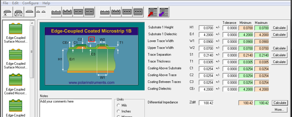
Impedance Calculation Methods and Tools
PCB designers use
a range of techniques to calculate the impedance of pcb traces, improve design methods, and maintain impedance control in pcb manufacturing. These tools and calculation techniques are at the heart of defining the required unique impedance for each signal:
- Online Impedance Calculators:Many PCB fabricators provide free controlled impedance calculator to calculate controlled impedance trace width based on the selected stack-up, trace width, height and materials. These calculators provide quick width estimates for trace and space.
- Field Solvers and Simulation Tools:The utilization of electromagnetic field model solves a high accuracy prediction of impedances in high frequency for advanced tools, such as Polar Si9000, Altium Designer, HyperLynx, in the presence of complex shapes and multiple dielectric layers.
- SPICE Simulators:These are employed to model transmission lines and impedance matching to observe transient responses and foresee possible problems of signal speed and integrity.
- Manual Equations:For less complex boards, the impedance of PCB traces can be calculated by applying classical microstrip or stripline equations with design parameters like trace width, dielectric constant, and trace height.
Example Calculation Table
Tool/Method | Best For | Accuracy | Speed | Ease of Use |
Online Calculator | Standard Stack-ups | Moderate | High | Very Easy |
Field Solver | Complex, multilayer boards | High | Medium | Moderate |
SPICE Simulator | Dynamic signal behavior | High | Low | Moderate |
Manual Equation | Initial estimates, education | Low/Medium | High | Easy |
Good PCB design techniques use these tools not just to create impedance estimates, but to verify and refine the trace dimensions and locations throughout the design process. This leads to well-controlled impedance, uniform impedance, and eliminates uncontrolled impedance risks.
Impedance Control Verification and Testing
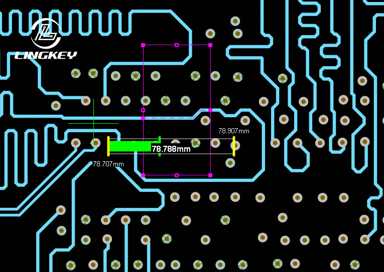
Post-fabrication inspection of PCBs is necessary as the real PCB layout may be quite different from the designed one because of process variables and manufacturing tolerances. That’s why your test coupon is a section of PCB – fabricated with your boards – that you use for accurate impedance testing. This coupon is a PCB that is meant to be used only for measurements, and that ensures that the results are that of process realities.
Time-Domain Reflectometry (TDR) and Test Coupons
A TDR is used to measure reflections along a test coupon to verify impedance is equal to expected values. For instance, if your controlled impedance signals need to be 100 Ω ± 10%, a TDR tells you whether each coupon is a PCB that lies within that window. This method detects any change in impedance and enables manufacturer and designer to avoid signal integrity problems prior to population and system integration.
Importance of Continuous Measurement and Documentation
- Create impedance verification routines:Every board revision should include updated test coupons.
- Impedance measures for all critical nets:Not just high-speed, but any circuitry on the PCB with impulse or RF waveforms.
- Comparison of design and production:Ensures the actual impedance on the PCB matches predictions from simulation and calculation.
Applications of Controlled Impedance PCBs
Controlled impedance is now standard in many fields where high-speed data, RF, or sensitive analog signals are present. Applications include:
- High-Speed Digital and Data Communication:PCIe, DDR, HDMI, USB, and networking hardware rely on uniform impedance.
- RF and Microwave Systems:Impedance signals guide power through antennas, filters, and amplifiers.
- Automotive and Aerospace:Today’s automotive electronics, radar, and avionics need reliable trace pairs for critical signals.
- Medical Devices:Imaging systems, diagnostics, and high-speed sensor require extremely low signal distortion and predictable circuit’s impedance.
- Consumer and Industrial Electronics:Any device where fast, error-free digital data is sent down PCB signal traces.
Key Features of Advanced Controlled Impedance PCBs
The most advanced printed circuit board fabrication services offer:
- Precision impedance control, often within ±5%.
- Support for a wide range of impedance levels:Single-ended (50 Ω, 75 Ω), differential (90 Ω, 100 Ω, or custom).
- Custom stack-ups, trace dimensions, and substrate material selection.
- Test coupon inclusionon every panel for in-situ TDR verification.
- Reporting and compliance documentation:Traceability for every production lot.

Impedance Control Design Checklist
A pragmatic advice for all PCB designers, so that they can expect repeatable and reliable signal behavior from every design:
- Identify all nets that require controlled impedance.
- Clearly annotate impedance signals in the schematicand documentation.
- Calculate and specify trace dimensions and locationsfor each relevant signal.
- Define precise impedance levelsin your fabrication notes (e.g., “90 Ω differential pairs, Layer 3, ±8%”).
- Specify stack-up and controlled dielectric material data.
- Design and request a test coupon—a PCB used to verify both single-ended and differential traces.
- Review outputs from all design calculation toolsbefore release.
- Communicate with the PCB fabrication team, sharing intent, tolerances, and critical nets.
- Interface with quality control on test coupon TDRs to confirm successful production.
FAQs: Impedance Control in a PCB
What determines the impedance of a PCB trace?
Why might actual PCB layout differ from simulated design?
Why is controlled impedance critical for signal integrity?
What is a test coupon and how is it used?
Can I control the impedance on all layers?
Conclusion
Needless to say, impedance control is a very critical element in PCB design. If you are working on high end communications product, RF sub system or high density digital circuit, controlled impedance ensures that high speed, low noise signals flow predictably, allowing designer to stay away from SI problems which arise from uncontrolled layouts. Through the use of transmission line theory, trace geometry and material properties, and by utilizing current impedance calculation and simulation techniques, the PCB designer can be assured that impedance is controlled from initial concept through final fabrication and testing.
Following good PCB design guidelines, providing clear manufacturing documentation, having well defined impedance requirements, including test coupons and simulating critically nets helps reduce the potential for signal integrity problems. If you control impedance, you control the performance and long term reliability of your electronics products.
Are you set to guarantee excellent signal quality in your next project? With a high speed pcb manufacturer like LingKey – providing controlled-impedance fabrication, engineering assistance and rigorous quality check, the high-speed design intent can be easily translated into uniform, production-ready pcb performance. Contact our engineers for a full design review or get a quote for your high-speed, controlled-impedance PCB solution today.
")
")


")
")
")


