PCB Gold Finger: Complete Guide to PCB Gold Fingers & Beveling
Table of Contents
ToggleIntroduction to PCB Gold Fingers
Reliable connectivity is the basis of nearly all modern electronic devices, and nothing illustrates that better than the gold fingers on a printed circuit board (PCB). these miniature, gold-plated connector pads (also referred to as gold fingers) play an essential role in maintaining optimal electrical connections in everything from industrial machinery to consumer electronics and medical instruments.
This all-rounder of the PCB gold finger covers their purpose, design, material, surface treatment such as Electroplated Hard Gold and ENIG (Electroless Nickel Immersion Gold), typical errors and the current modular system trends in the field of computer hardware, telecommunication, and industrial automation. Whether you are an engineer or a buyer, After reading this article you’ll understand why gold fingers are used, what quality looks like, and how to maximize signal integrity and wear resistance.
What Are PCB Gold Fingers?
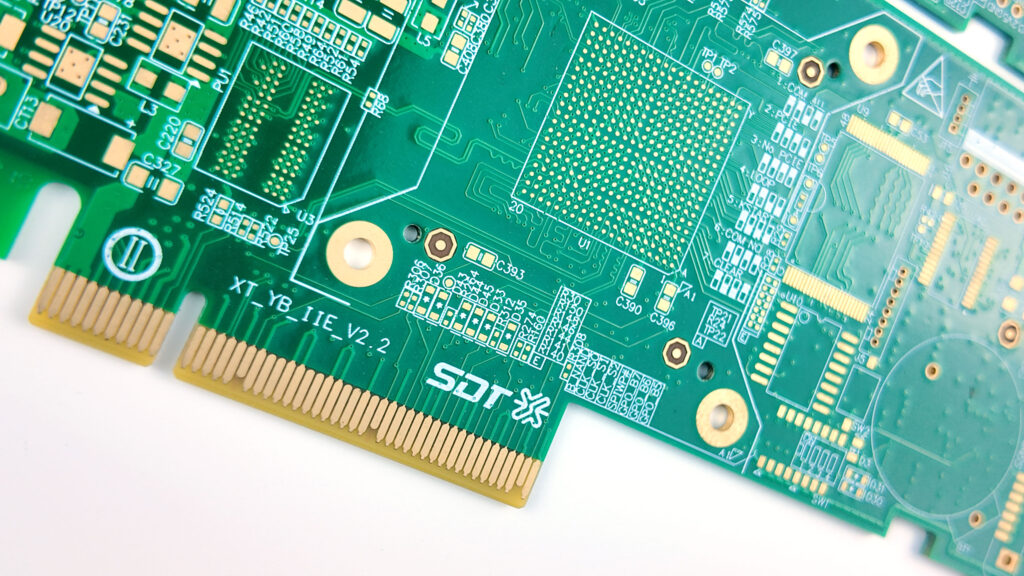
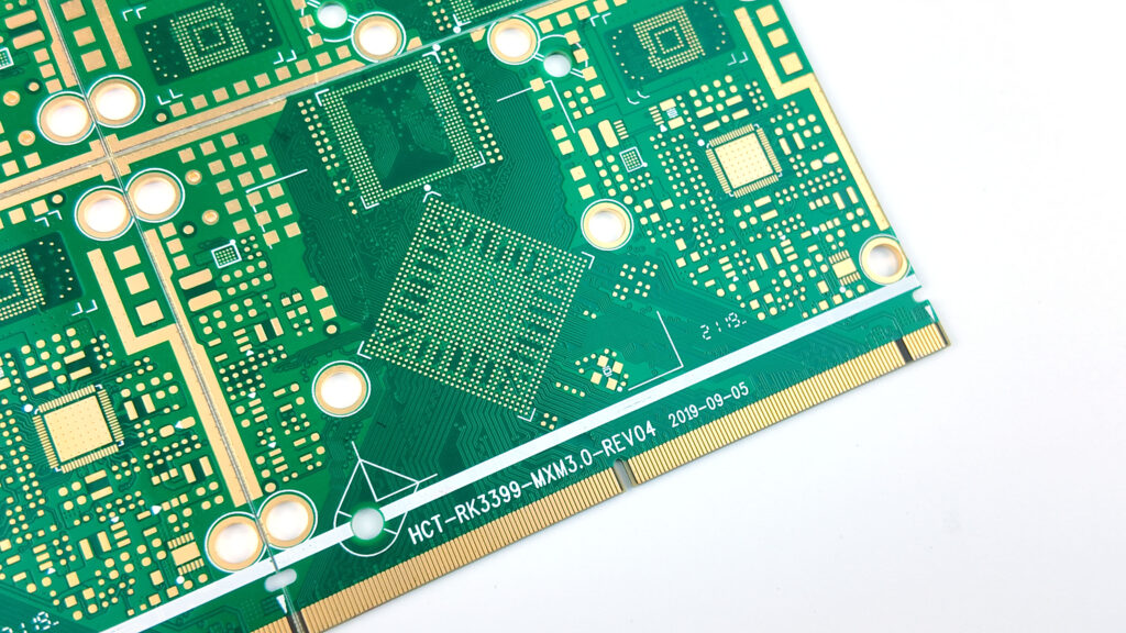
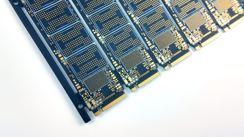
PCB gold fingers are turned, gold-plated edges on the edge of a printed circuit board. They are conductive contacts, connecting two surfaces, such as two PCBs or a PCB and an edge connector in a modular or plug-in assembly. These traits are especially prevalent in applications where PCBs are frequently mated and unmated (eg memory modules, expansion cards, or network equipment).
Structure and Materials
- FR4 Material:The standard base for most PCBs, providing strength and insulation.
- Copper Traces:Carry current throughout the board.
- Nickel Underlayer:Acts as a reliable barrier to improve gold adhesion and prevents copper migration, enhancing corrosion resistance.
- Gold Plating:Provides the actual contact surface, offering both conductivity and incredible wear and corrosion resistance for high-cycle, plug-and-play use.
The Purpose of Gold in Edge Connectors
The reason for using gold for PCB gold fingers is that it has the best conductivity and resistance to corrosion. Stable electrical connections are critical in sectors where the connectors are constantly plugged and unplugged—including industrial control systems, computer hardware, and communications gear. The chemically stable nature of gold can ensure connector performance in the harsh environment or in humid weather, and the low contact resistance of gold can enable signal stabilization with the least signal loss.
Why Gold?
- Exceptional Conductivity:Ensures signals are transmitted with minimal resistance.
- Corrosion Resistance:Withstands oxidation and moisture, critical for telecommunications infrastructure and automotive electronics.
- Wear Resistance:Gold fingers maintain low contact wear even after thousands of plugging cycles.
- Reliability in Modular Systems:Guarantees secure, hot-swappable, and long-term connections.
Types of Gold Fingers in Printed Circuit Boards
When talking about the kinds of gold fingers for pcb production, it is related to both structural difference and surface treatment difference. The selection is governed by the application, connector type, and assembly process.Structural Differences.
Structural Variations
- Standard/Flush Gold Fingers:Even alignment; general use in edge connector systems.
- Uneven Gold Fingers:Different lengths for sequenced or staggered connections.
- Segmented Gold Fingers:Divided finger groups for multi-channel systems or isolated circuits.
Surface Treatment Types
- Electroplated Hard Gold:Utilizes the electroplating process to deposit a thick, hard, wear-resistant gold layer suitable for high-cycle connections—standard in memory modules, PCBs in industrial equipment, and automotive electronics.
- ENIG (Electroless Nickel Immersion Gold):This finish, using a chemical (electroless) rather than electroplating process, provides a thinner but much more uniform gold layer, ideal for high-density interconnect (HDI) boards and situations where solderability and surface finish are important.
Type | Gold Thickness | Wear Resistance | Typical Application |
Electroplated Hard Gold | 1–50 μm | High | Expansion cards, RAM, connectors |
ENIG | 0.05–0.1 μm | Moderate | HDI, IoT, wearables, small connectors |
PCB Gold Fingers vs. PCB Edge Connectors
While often used interchangeably, the terms gold fingers and edge connectors are technically distinct:
- PCB Gold Fingers:The gold-plated contact fingers found on the edge of a PCB. They serve as the interface for electrical connections.
- PCB Edge Connectors:The actual mating connectors, often sockets or slots, that accept the PCB gold fingers for a reliable, repeatable connection.
Comparison Table
Feature | PCB Gold Fingers | PCB Edge Connectors |
Location | On PCB edge | On motherboard or enclosure |
Main Material | Gold plating on copper | Plastic/metal (with contacts) |
Role | Provide connection interface | House and electrically connect gold fingers |
Cycle Life | 5,000–50,000+ | 5,000–50,000+ |
Gold Finger Beveling and Chamfering
But beveling (or chamfering) is also important in the assembly process for gold fingers, even if it is often ignored. It is ground with the insertion edges on an angle, usually 30° or 45° to enable a smooth, no-damage mating with edge connectors.
Benefits of Chamfering/Beveling
- Prevents Mechanical Damage:Reduces abrasion during connector insertion.
- Improves Connector Life:Less strain on both gold fingers and the edge connector.
- Essential for High-Density Designs:Beveling is particularly beneficial for compact, high-density interconnect (HDI) PCBs where tight tolerances are critical.
Plating Thickness, Gold Plating, and Surface Treatments
Gold Plating Types & Thickness
The thickness of plating greatly affects both the quality and the life of the PCB gold fingers. Electroplated hard gold and ENIG (Electroless Nickel Immersion Gold) are used, each has its own advantages.
Common Plating Thickness Standards
Application Area | Typical Plating Thickness | Surface Finish |
Consumer Electronics | 0.76–1.27 μm | ENIG/Hard Gold |
Computer Hardware | 1.27–2.54 μm | Hard Gold |
Industrial/Automotive | 2.54 μm+ | Hard Gold |
Nickel Layering: Between the copper substrate and the gold surface, nickel acts as a barrier to stop the migration of copper, which preserves the high conductivity and reliability of the gold.
Surface Treatment Methods
- Hard Gold (Electroplated):For maximum wear resistance.
- ENIG:For fine-pitch, low-wear, HDI and IoT applications.
- Combined Surface Treatments:Some sophisticated PCB fabrication can employ a combination and have hard gold in high wear and high contact areas and ENIG on the rest of the board to be more economical and sn1100 solderable.
- Quality Fact:Gold finger surface finish should be tested for thickness, purity and adhesion for electrical performance and to comply with industry quality standards (such as IS/IEC, ASTM, UL, ISO etc.) as applicable per.
Manufacturing Process for High-Quality Gold Fingers
The precision and performance of gold finger PCBs are directly tied to their manufacturing process. Each step is designed to preserve conductivity, corrosion resistance, and wear resistance.
Typical Assembly Process
- Design and Trace Routing:Engineers specify the design specifications, including trace width, placement of connector pads, and surface finish requirements. Strict design guidelines are followed for optimal signal integrity and mechanical strength.
- Preparation and Solder Masking:The FR4 material board is cleaned, and solder mask is applied to protect non-finger areas, leaving the future gold fingers exposed.
- Nickel Plating:A nickel underlayer (generally 3–8 µm thick) is applied to prevent copper diffusion into the gold and reinforce the connector pads.
- Gold Plating:Hard gold plating (via the electroplating process) or ENIG is deposited on the nickel. The gold thickness and uniformity directly affect durability and electrical performance.
- Beveling Process:Chamfering angles (30° or 45°) are machined to create smooth, reliable connection interfaces, as specified by the edge connector mating component.
- Surface Finish and Conformal Coating:Steps are taken to ensure the final surface finish is uniform and free from contaminants. In some high-performance applications, an optional conformal coating is added for protection.
- Quality Control:Every batch undergoes electrical testing, visual inspections, plating thickness measurement, and wear tests, adhering to IPC standards and requirements for RoHS and REACH compliance.
Enhancing Reliability Through PCB Gold Finger Beveling
Beveling of the PCB gold finger is one of the important component of gold finger design. This stage of production is the one that enables grinding and angling of the gold finger pcb ends to a specific angle—typically 30, 45 or higher degrees. PCB gold finger beveling is not optional but a vital standard for PCB gold fingers established by professional body such as IPC since it has a huge impact on the wear properties, insertion feel and long term reliability of every modular connection interface.
Why Is PCB Gold Finger Beveling Essential?
- Prevents Damage:The beveling process prevents direct edge-on collisions with mating contacts in edge connectors, which can otherwise scrape off the gold plating.
- Extends PCB Life:With regular use, the use of gold fingers involving proper beveling maintains a smoother engagement, furthering the cycle life for plug-and-play devices and high-performance applications.
- Supports Signal Integrity:Proper PCB gold finger beveling aligns the connector pads correctly, maintaining integrity even in high-density and high-frequency trace routing environments.
Precision Matters: Achieving the Right PCB Gold Finger Plating
Meeting gold finger specifications begins with the right choice and thickness of PCB gold finger plating. Manufacturing high-quality gold fingers requires the plating process to be controlled down to the micron, typically ranging from 0.76 μm for basic consumer electronics up to 2.54 μm or more for industrial or automotive systems.
Why Strict Plating Specifications Matter
- Improved Wear Resistance:The thicker the PCB gold finger plating, the higher the mechanical life—vital for expansion cards and industrial equipment where gold fingers are used extensively.
- Stable Conductivity:Uniform plating ensures consistent performance. Uneven surfaces or insufficient thickness is a common cause of premature connector failure.
- Meets Industry Standards: Adhering to accepted standards for PCB gold fingers (IPC, ASTM, UL, ISO, RoHS, REACH) is the only way to guarantee compliance in regulated sectors
Gold Finger Plating in Action
In high-end memory modules, the use of gold fingers with plating thickness over 2.54 μm doubles wear resistance, offering superior electrical performance even after thousands of insertions. This is why gold fingers used in such applications are always specified with exact plating thicknesses and inspected for compliance.
Gold Finger Design: Rules and Specifications
Precision gold finger design is one of the first steps in manufacturing high-quality gold fingers. It incorporates every detail, from physical dimensions to the tiniest details of the surface finish.
Key Elements in Gold Finger Design
- Gold Finger Specifications:Each aspect of the finger (width, length, gap, bevel, plating) must follow industry design standards for PCB gold fingers.
- Trace Routing and Edge Placement:Traces must feed reliably into the connector pads, ensuring low impedance paths for high-speed signal processing.
- Solder Mask Clearance: Adequate clearance is vital—overlapping the solder mask on gold finger PCB regions can obstruct conductivity.
Rules of PCB Gold Fingers
- Define proper beveling angles for all insertable edges.
- Specify plating thickness for gold finger PCB based on cycle life and application.
- Document all surface treatment choices and material stack-ups.
- Design for the correct pad spacing and connector requirements.
Design Example Table:
Rule | Standard Value | Real-World Use Case |
Beveling Angle | 30° or 45° | PCI Express & RAM modules |
Gold Plating Thickness | 1.27–2.54 μm+ | Automotive, mission-critical interfaces |
Pad Gap | ≥0.30 mm | Telecommunications infrastructure |
Solder Mask Clearance | ≥0.50 mm | Medical device edge connectors |
Why Gold Fingers Are Used—and Why the Use of Gold Matters
The dominant use of gold fingers across printed circuit boards and edge connectors is driven by the unique use of gold as a surface finish. Not only does the use of gold maximize electrical performance and signal integrity, it also separates high-quality products from short-lived, unreliable alternatives.
Where Are Gold Fingers Used Most?
- Modular plug-in boards for network and control systems.
- Removable memory and storage cards in consumer electronics.
- All high-cycle connection interfaces in automotive and industrial automation.
The Ultimate Purpose of Gold
- Electrical Stability:Gold keeps resistance low and stable over time, especially when modular systems require frequent connection and disconnection.
- Maintenance-Free Life:Products with gold finger PCB interfaces require minimal cleaning and have unparalleled corrosion resistance.
- Signal Quality:In advanced telecommunications, medical devices, and aerospace applications, signal loss and poor connections are simply unacceptable.
Benefits of PCB Gold Fingers: Conductivity, Durability, and Signal Integrity
PCB gold fingers are chosen for several key advantages:
- Outstanding Conductivity: Enables robust, high-quality signal transitions and stable power draw for the adaptors.
- Superior Wear Resistance: Electroplated surfaces can withstand tens of thousands of connection cycles.
- Corrosion Resistance: Gold never tarnishes, and it outlasts tin or silver in humidity or in industrial or marine atmospheres.
- High Signal Integrity: Provides clean, robust signal paths, a must for telecommunications, IoT/wearables, and signal-processing applications.
- Easy Modular Design: Enable hot-swapping as well as modularization for ease of maintenance and future upgrades.
- Support for High-Density Interconnect (HDI): Important as device dimensions shrink and pin per inch requirements increase.
Challenges, Environmental Concerns, and Technological Advances
Challenges in manufacturing high-quality gold fingers include:
- Cost:Gold is precious; its use increases PCB cost and requires optimized design.
- Environmental Concerns:Gold mining and chemical processing are not always eco-friendly, though RoHS and REACH compliance and new recycling methods help mitigate impact.
- Design Constraints:As PCBs shrink, keeping sufficient gold finger area for safe high-speed connections can be difficult.
- Precision Required: Plating, beveling, and pad alignment must be flawless for signal integrity and mechanical life.
Recent Technological Advances
- Improved Electroplating Processes:Deliver finer, more uniform gold finishes and reduce environmental waste.
- Material Research:New alloys and finishes aim to provide similar performance at lower cost.
- Enhanced Conformal Coatings:Better protection and longevity even in aggressive environments.
- HDI and Fine-Pitch Improvements:Enabling dense, reliable connectivity for wearables, smartphones, and next-gen computing.
Common Design & Manufacturing Mistakes to Avoid
- Using gold plating of insufficient thickness for high-cycle connectors.
- Permitting the solder mask to encroach on the connector pads.
- Omitting or botching the beveling/chamfering process.
- Not checking for conformance to the IPC and the international standards.
- Pollution or contamination controls were disregarded in the plating and in the assembly.
Quality Control, Compliance, and Testing
A trusted Gold Finger PCB needs to undergo strict QC at all the processes, from sourcing of raw materials to the finished product assembly.Leading manufacturers adhere to :
- IPC-6012, IPC-A-600, ASTM, UL, ISOcertification guidelines
- Electrical Testing: Continuity and resistance checks
- Visual & Dimensional Analysis: Checking for cracks, voids, misplates
- Plating Thickness Measurement: Ensuring adherence to design standards
- Wear and Insertion Testing: Verifying mechanical durability and electrical performance over repeated cycles
Frequently Asked Questions (FAQs) About PCB Gold Fingers
Why are gold fingers used in PCBs?
What types of gold plating are used?
How thick should gold plating be?
Are there environmental concerns with gold fingers?
What is the role of nickel underlayer in gold finger PCBs?
Final Thoughts on Manufacturing High-Quality Gold Fingers
From the process of PCB gold finger beveling, to the gold finger plating in thickness that’s tightly controlled, and finally the compliance with the newest spec for the PCB gold finger, every step is very important in the manufacturing of usable gold fingers that your products—and their users—can count on. In any application in which gold fingers are involved, you can be certain that that strict gold finger specifications, industry standards, and proven design rules have been followed to help you design-in the durability, reliability, and signal quality your cutting-edge electronics products demand.
Whenever a new product incorporates gold fingers, it’s worthwhile to start with the comprehensive guide to PCB gold finger design—making sure each connector in your product lives up to the gold standard. And keep this in mind: it’s the presence of gold in these connectors that enables them to hold up to thousands of cycles and drive modular high-performance electronics racing ahead in just about every field.
Conclusion
PCB gold fingers continue to be essential to the operational success of many modular, high-reliability, and high-density electronic systems. This allows a printed circuit board (PCB) to provide consistent conductivity, resist corrosion, enable HDI and modular design, and go through tens of thousands of connections in control systems, network equipment and beyond.
Optimal results are achieved by selecting the appropriate gold finger type, adhering to uncompromising design standards (IPC, ASTM, UL, ISO, etc.), and demanding the same level of stringent quality assurance and environmental compatibility throughout the pcb assembly process. For the high-end, high-performance, future-proof use case, gold fingers are, and will stay, the gold standard
")
")


")
")
")


