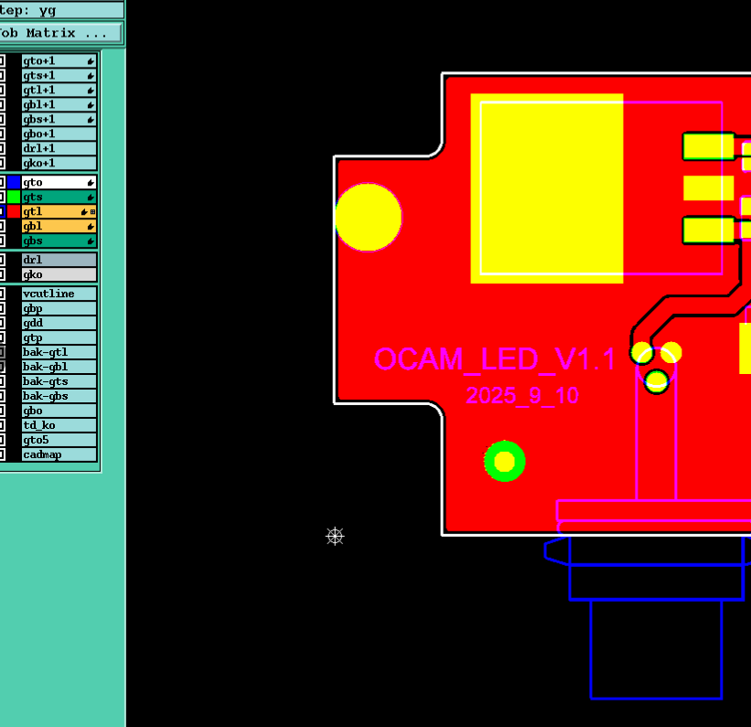
Optimize gerber data
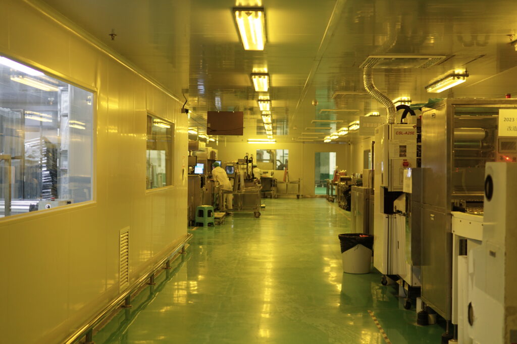
Production material preparation
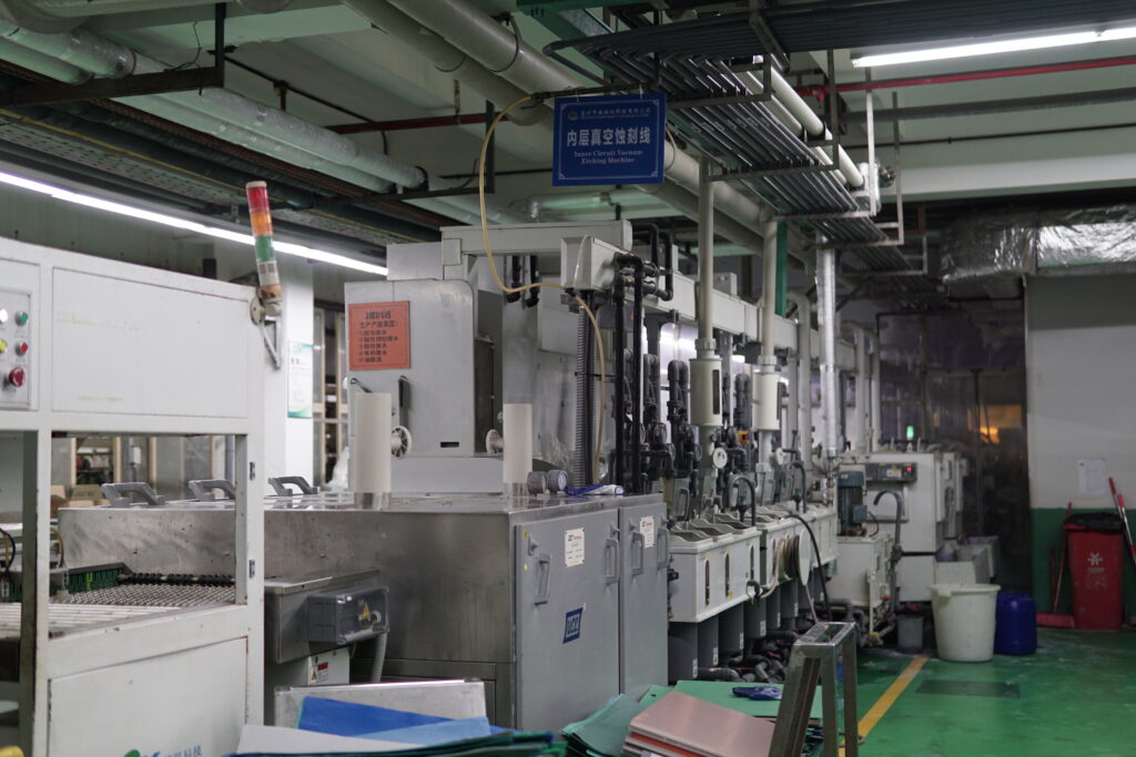
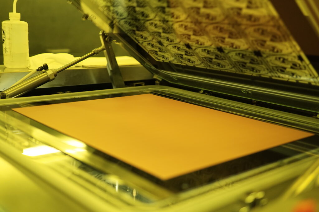
Inner layer circuit
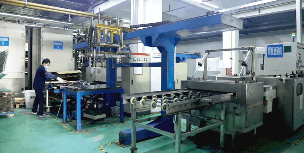
Lamination (applicable to multi-layer PCB boards)
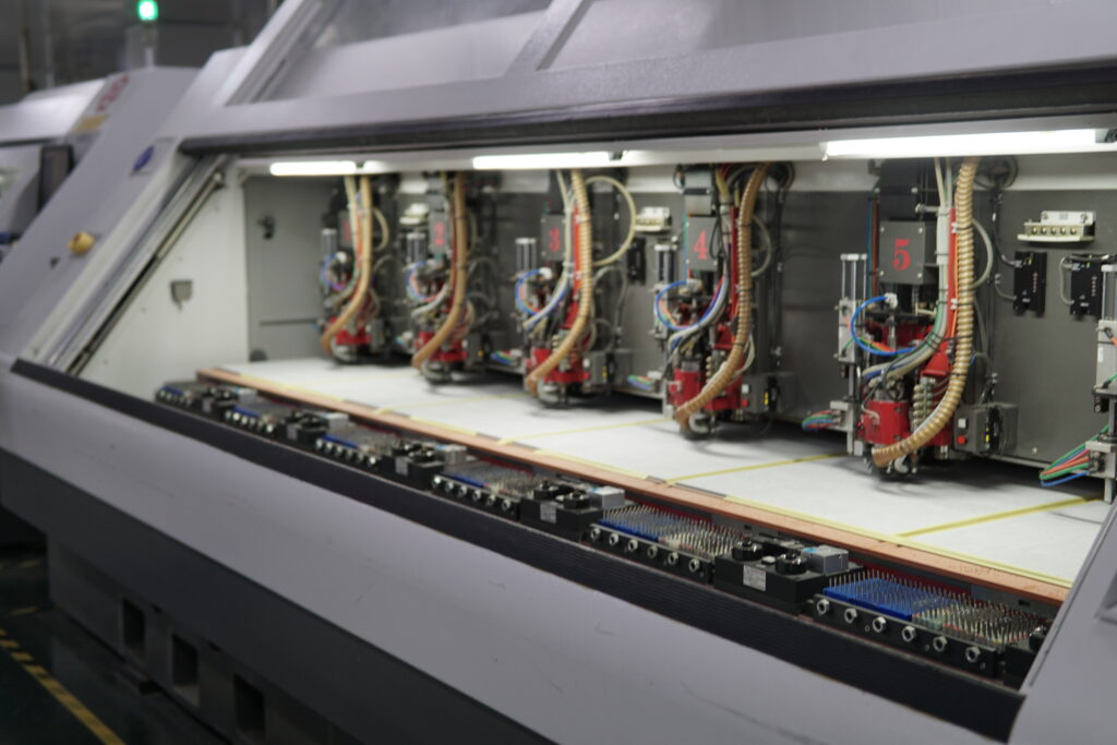
Drilling
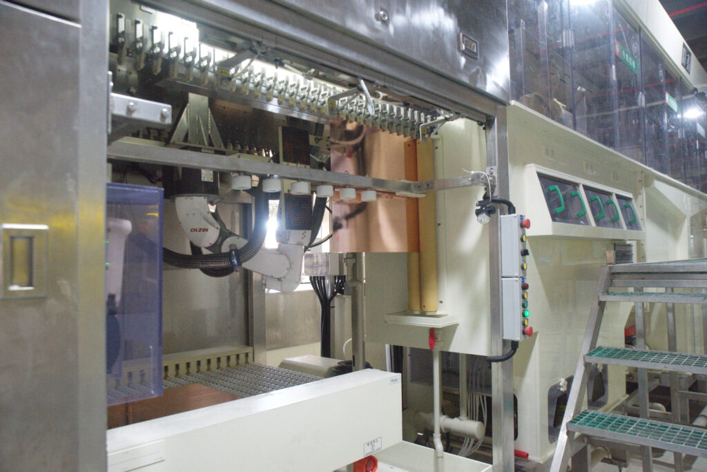
Copper deposition
Outer layer circuit
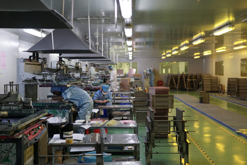
Printing solder mask and silk screen
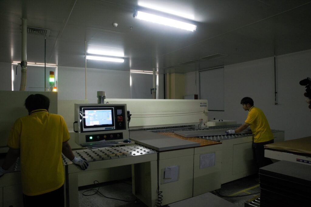
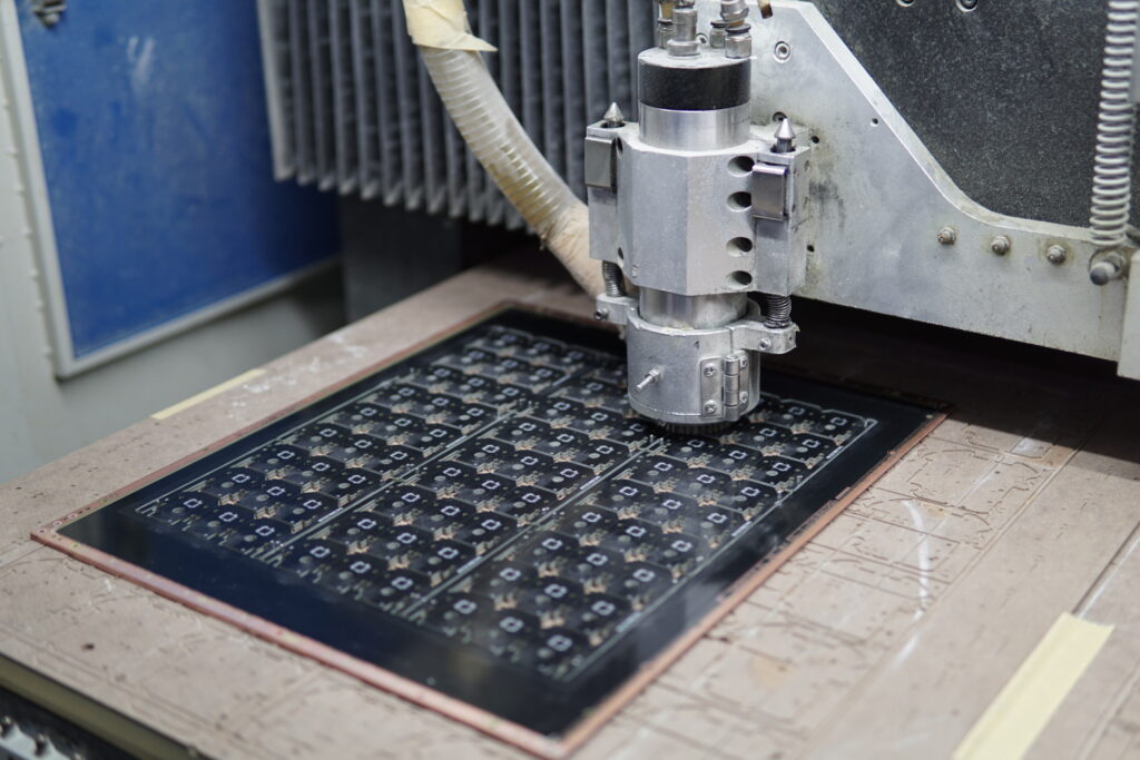
Surface treatment, and cutting the whole circuit into unit pcb
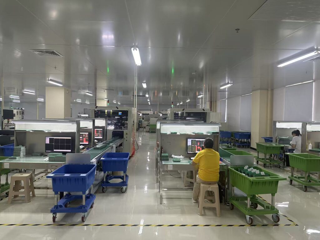
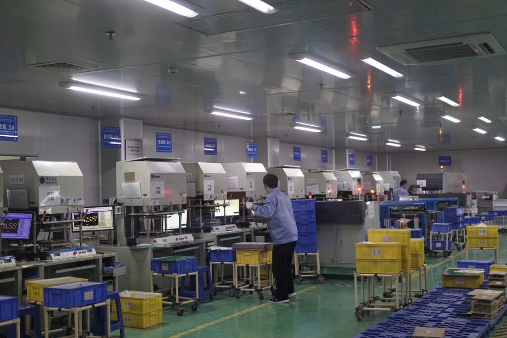
Electronic testing and FQC
Packaging and transportation