Tombstoning in PCB Assembly: Causes and Solutions for Tombstone Defects During Reflow Soldering
Table of Contents
ToggleIntroduction
Tombstoning risk is now one of the largest problems the high-tech electronics industry is facing. With the increasing density of surface mount components on modern printed circuit board (PCB), engineers and designers are challenged by increasingly complicated assembly processes and escalating probability of defects such as tombstoning that directly influence reliability of electronic devices and the performance of the PCB. Tombstoning is a defect within the printed circuit board (PCB) that not only interrupts the working of the device but also increases the pcb manufacturing cost and stops the entire production line. In this article, we will analyze the nuances of tombstoning, including how and why it occurs, its effect on the assembly quality and, most importantly, prevention methods for PCB tombstoning to lead to high-quality PCB assemblies.
What is Tombstoning in PCB Assembly?
Tombstoning in PCB assembly is a phenomenon where one end of a surface mount device (SMD) resistor, capacitor, etc. rises into the air, standing on end like a gravestone, much like what is shown on the right in Figure 1. That situation generally happens in the reflow soldering process of the PCB assembly process, where one end of the part is raised off the board caused by the unbalanced heating or unbalanced wetting forces. Therefore, at that open end, the connection is disconnected, which can lead to an open circuit and threaten the reliability of PCBs as well as the functionality of an assembly device.
Key Features of PCB Tombstoning
- Primarily affects compact SMT components with two terminal ends
- Most likely to happen during the reflow process
- Results from the difference in solder wetting forces or thermal gradients acting on both sides of the component
PCB tombstoning usually happens during soldering when one side of a component is heated more than the other, or is given more solder. The rosin flux core is also critical to good electronics – a knowledge of and prevention of tombstoning in the rad-hole ensures that connections remain solid and that “open circuits” are minimized.
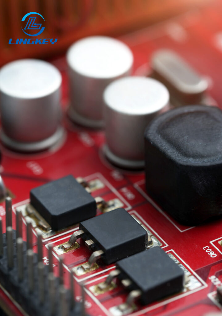
In SMT production lines like those at LingKey, tombstoning is actively monitored as a sign of thermal balance and proper solder wetting.
What Causes Tombstoning in PCBs?
The investigation of the causes and effects of PCB tombstoning is essential for establishing robust process rules in assembly. In this article, we will detail the most common causes19 among the pcb production industries.
Common Causes of PCB Tombstone
Cause | How It Contributes |
Imbalance in Solder Paste Volume | Variability in solder paste application or stencil design leads to more solder on one side |
Thermal Gradient Variations | Uneven heating means one pad melts solder faster, causing the component to stand up |
Pad Design and Surface Finish | Pad size, shape, or poor finishes (e.g., HASL vs. ENIG) affect solder wetting |
Component Placement Challenges | Misalignment increases the likelihood of tombstoning during reflow |
Component Geometry and Size | Smaller devices or those with irregular terminals are more susceptible |
Material Properties and Surface Tension | Poor solder paste rheology or PCB contamination distorts wetting forces |
Board Warpage and Flatness | Warped boards reduce uniform contact, raising tombstone risk |
Solder Paste Type and Reflow Profile | Incompatible paste or poorly profile during reflow soldering fosters defects |
Producers like LingKey usually consider these causes together, since tombstoning is more of a multi-faceted process issue rather than a single point of failure.
Causes Warranting Special Attention:
- Imbalance in Solder Paste Volume: Uneven solder application—often because of worn or poorly designed stencils—leads to a quantity of solder paste that differs with each pad, so a uniform application of solder paste plays a critical role in prevention of defects.
- Thermal Gradient Variations: A non-uniform temperature on the PCB in the reflow oven can cause solder to liquefy at different times at each end (side of the component to the other side). The result is the infamous “see-saw” vibration or vertical chip migration.
- Pad Size and Surface Finish: To reduce tombstoning, the IPC-recommended pad geometries, smooth surface finishes (like ENIG) and omission of HASL for small-pitch components are vital.
- Solder Wetting and Material Properties: Working with material vendors to develop solder pastes that improve solder wetting and adhesion is important.
The Impact of Tombstoning PCB Defects
Tombstoning effects are not limited to cosmetic defects, but are also related to the reliability of the electronic device and the PCB performance.
Consequences of PCB Tombstoning
- Device Failure: The most immediate effect is the open circuit—making a resistor or capacitor non-operative and potentially leading to device failure.
- Reduced Reliability: Even a momentary break in contact can reduce the reliability of PCBs in critical applications such as medical devices, automotive systems, or aerospace.
- Increased Production Costs: Rework and scrap increases lead times and costs for high-quality pcb assemblies.
- Quality Metrics: As can be seen in the following table, high rates of tombstoning degrade essential quality factors.
Quality Metric | Without Tombstoning | With Frequent Tombstoning |
Assembly Yield | High (>98%) | Reduced (85-95%) |
Reliability of Electronic | High long-term stability | Frequent failures, lower confidence |
Overall Performance | Optimized | Degraded, additional manual steps |
Production Cost | Minimized due to less rework | Increased due to scrap/rework |
How to Prevent Tombstoning PCB Defects
Prevention is always better than cure when it comes to printed circuit board assembly. Safe stops for PCB tombstoning include design, material, and process controls, each of which is essential in the delivery of high quality PCB.
Design-Focused Approaches
Optimize Pad Layout
- Adhere to IPC-7351 for balanced pcb pads
- Avoid oversized pads and ensure proper spacing according to component geometry
Surface Finish Selection
- Prioritize ENIG or OSP for uniform solder wetting
- Use SMD pads to further enhance attachment
DFM Collaboration
- Early involvement of manufacturing and process teams avoids tricky layouts or at-risk footprints
Materials and Stencil Management
Uniform Solder Paste Application
- Use high-precision, laser-cut stencils to ensure uniform solder pasteacross all pads
- Specify step-down apertures for small, sensitive SMT components
Material Suppliers to Develop Solder Pastes
- Collaborate with reputable material suppliers to develop solder pastes tailored for your application
- Choose pastes that enhance solder wetting and adhesion
Process and Assembly Controls
Refined Soldering Techniques
- Profile every board and component type; tune oven settings for even ramp and soak stages
- Ensure that thermal masses are balanced, so one end of the componentis not heated ahead of the other
Precision Placement
- Maintain tight calibration of pick-and-place equipment
- Apply x, y, theta compensation as needed
Address Board Warpage
- Use high-quality, low-warp materials and proper storage
Inspection—AOI and Manual
- Integrate Automated Optical Inspectionto identify defects quickly after the reflow process
Best Practices Checklist
- Use IPC-compliant pad layouts and finishes
- Ensure uniform solder paste application with precise stencil design
- Regularly profile ovens for thermal uniformity
- Optimize reflow settings for balanced heating
- Collaborate with suppliers to develop solder pastes fit for purpose
- Continually train assembly staff for best practices and defect recognition
Effective Solutions for Addressing Tombstoning PCB
Despite best preventive efforts, tombstoning requires practical corrective measures when it appears.
Process Adjustment
Strive for a synchronized melting of the solder at both ends of surface-mount components by adjusting the reflow soldering process. This is particularly important in minimising the risk of tombstoning (flip up of one end of an SMT component) mainly for precision SMT components (resistors and capacitors). Good reflow temperature profiling and control of thermal balance is the basis for the elimination of tombstoning defects.
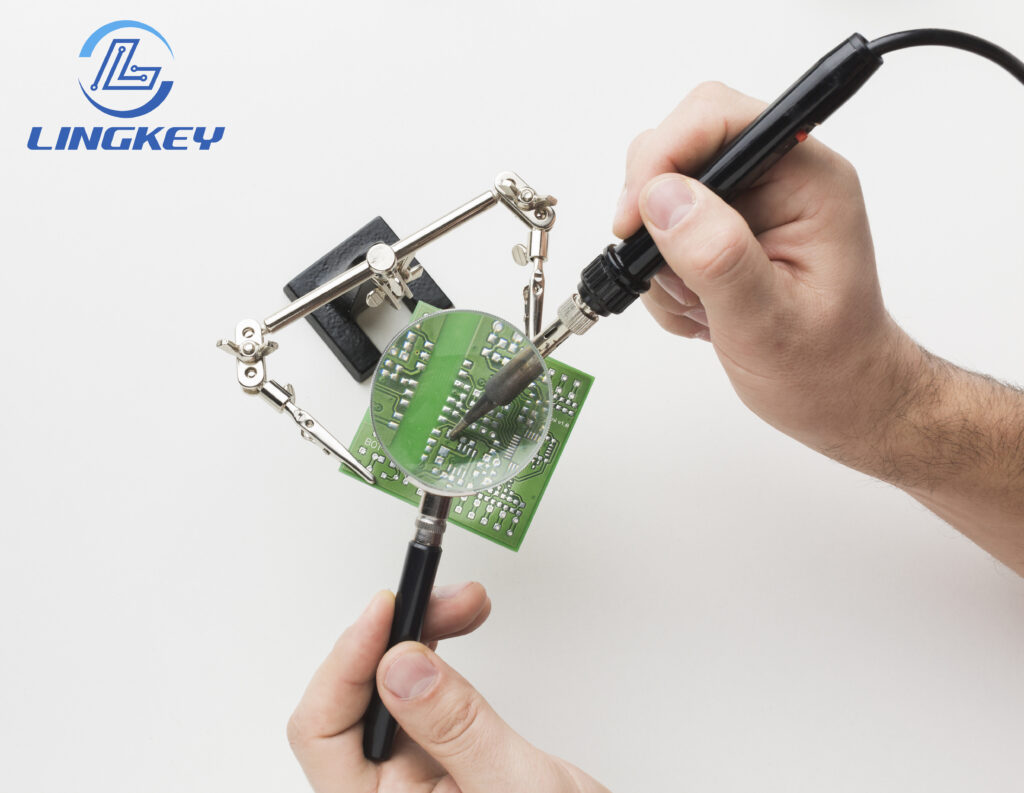
Skilled Manual Rework
When post-reflow a PCB tombstoning is found directly skilled technicians rework manually with fine tip soldering irons and magnifier. Heating of the adjacent parts is avoided and quality of high-end PCB assemblies is preserved. Manual rework consist in re-flowing the solder joints and re-aligning the lifted components so that both terminals make solid contact with the pads, regaining full circuit functionality and the reliability of the electronic devices.
Continuous Quality Improvement
Cultivating a culture of continuous quality improvement is essential. With this insight into how often and what causes tombstoning-inducing events, manufacturers can detect patterns and evolve their practices. Incorporating statistical process control, equipment upgrades, and re-education of personnel in soldering techniques can result in continual improvement in production process defects.
Advanced Inspection and Testing
The in-line AOI equipment can catch tombstoned parts right after the reflow soldering process. The AOI systems quickly analyze the full populated board to a programmed reference, and any defects are identified and flagged for repair or to be used as feedback to process optimization.
Collaborating With Material Suppliers
Collaborate closely with your material suppliers to develop solder pastes tailored to your assembly environment, which can be a key factor in tombstoning avoidance. Material scientists can adjust flux chemistry and alloy compositions to provide uniform melting, improved solder wetting and adhesion, and reduce differential wetting stress which may induce components to stand vertically.
Innovative Rework and Assembly Techniques
Certain high-reliability industries use selective local heating, for example focused hot air nozzles or low-power laser reflow to rework tombstoned parts on high density boards without affecting surrounding SMT parts. These advanced soldering methods make it possible to avoid tombstoning in the initial assembly and during post-process repair.
Frequently Asked Questions (FAQ) About Tombstoning PCBs
Can uniform solder paste application alone prevent tombstoning?
Why is tombstoning more common with smaller SMD passives?
How does board warpage increase the risk of tombstoning?
What’s the difference between HASL and ENIG surface finishes in terms of tombstoning risk?
What role do material suppliers play in tombstoning prevention?
Conclusion: Minimizing Tombstoning for Reliable PCBs
The ability to predict and manage the risk of tombstoning is critical in the production of both high-quality PCB assemblies and the long term reliability of electronic devices. When the entire process is considered from an assembly standpoint—including uniform solder paste coverage, integrated pad/stencil design, equalized thermal profiles, and material supplier cooperation—tombstoning incidents can be greatly minimized. Routine monitoring with AOI, professional manual rework and a mentality towards process improvement continue to bolster the quality and reliability of the end product.
With the support of professional PCB assembly vendors like LingKey, process control and design collaboration can be effectively leveraged to minimize the risk of tombstoning in today’s SMT manufacturing.
In conclusion, careful design, process control, and supplier partnerships are essential in preventing tombstoning and delivering high quality PCB As and Bs that protect your brand and delight your customers.
")
")


")
")
")


