Ultimate Guide to PCB Antennas: PCB Antenna Design, Antenna Designs, Best Practices, and Antenna Types
PCB design has evolved to make transceivers more compact and robust by designing the antenna on the PCB board. For IoT, Wi-Fi applications or NFC applications, it’s imperative that engineers and innovators understand the science and the art of designing a PCB antenna . This in-depth look covers all the elements that make up a PCB antenna – the difference in material, layout considerations to attain good signal integrity, as well as the comparison with chip and flexible antennas.
Table of Contents
ToggleIntroduction to PCB Antennas
A PCB antenna has a radiating element which is printed on the PCB with other electronics. Unlike the isolated antenna or chip antenna (that is pre-manufactured and mounted as an external component) the PCB antenna is simply a pattern of copper traces which are etched on to one side of the PCB. This antenna functions by transforming the electrical currents in RF circuits into electromagnetic waves that propagate in free space.
Importance in Modern Communication Systems
PCB antennas are a key component in today’s communication systems, particularly with the increasing wireless connectivity requirements in portable and embedded systems. They are also popular in RFID, Wi-Fi and NFC applications as they facilitate product assembly by not requiring a separate antenna. This reduces not only the assembly cost, but also improves reliability by maintaining the signal integrity through a closer integration to the device’s RF design.
PCB Antenna Fundamentals and Theory
The size and shape of a pcb antenna affects its performance, as are the materials used to make it, the layout of the board, and the frequency at which it is designed to operate. PCB antenna designs are tailored to operate at assigned frequencies, where the antenna is required to radiate and receive energy effectively.
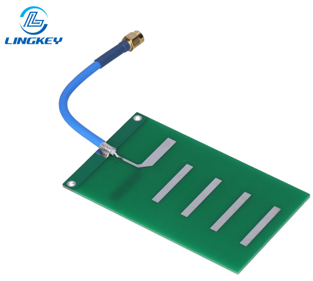
- Antenna on the PCB:The antenna type (monopole antenna, dipole antenna, patch antenna, slot antenna) affects not only frequency response but also the size, the structure and the ground plane.
- Signal Integrity:Good PCB design causes RF signals to be strong and clean, through the control of return loss, impedance and inadvertently coupling stray capacitance/gnd bounce.
- RF Design Considerations:The trace width, antenna, dimensions and position in relation to other traces/planes have an antenna and system impact.
Benefits and Limitations of PCB Antennas
Benefits
- Eliminating the Need for Separate Antennas:Printing the antenna directly on the PCB helps save space and cost.
- Scalability:Makes mass production of PCBs and their assembly easier since the antenna is just another pattern that is etched during production.
- Customization:The size and shape of the radiating element can be customized for any wireless protocol—Wi-Fi, Bluetooth, NFC, or LTE—to meet specific requirements for gain and bandwidth.
- Reliable Signal Integrity:The tight integration of the antenna with the RF circuit and the reduction in connectors and solder joints conserve RF performance.
Limitations
- Affect the Performance of PCB:Material choice, component proximity, and poor ground plane design are detrimental to antenna performance.
- Careful Design Required:The layout is very susceptible to the magnetic fields and coupling interference, thus meticulous design and simulation is required for hf and multi-protocol system.
- Tuning Challenges:PCB antennas cannot be retuned as easily as detached or flexible antennas once fabrication has been completed; it needs precise simulation and prototyping.
- Size of the PCB:Antenna performance may be constrained by space, particularly at low frequencies, where longer antennas are needed for resonance.
Types of PCB Antennas
Overview and Classification
On the modern PCB, you’ll encounter various PCB antenna types, each suited for particular tasks:
Type of Antenna | Description | Common Applications |
Monopole Antenna | Single conductor, often a straight or meandered trace | Wi-Fi, Bluetooth, general RF |
Dipole Antenna | Two symmetrical radiating elements | Basic wireless, reference antenna, IoT |
Patch Antenna | Flat, rectangular/circular, uses ground plane | GPS, Wi-Fi, compact IoT, reference design |
Slot Antenna | Slot cut in ground plane, substrate radiates | UWB, Wi-Fi applications, sensitive to magnetic fields |
Meandered/Inverted-F | Compact, folded design | NFC, wearable, RFID systems |
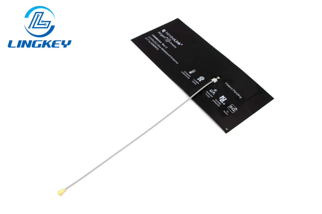
Flexible Antennas | Made with flexible PCB material | Wearables, foldable electronics |
Types include: loop, helical, and Yagi antenna systems. Among these, the patch, monopole, dipole, and slot antennas represent the most popular PCB antenna designs in the wireless consumer product industry.
Materials for PCB Antennas and Circuit Design
The Role of PCB Material
The PCB material—substrate in particular—defines many of the electrical factors that determine the behavior of an antenna. Parameters such as dielectric constant, substrate thickness and loss tangent have a direct impact on antenna efficiency and bandwidth.
PCB Material | Dielectric Constant | Applications |
FR4 | ~4.4 | Standard communication systems |
Rogers | 3.0–3.5 | High-frequency, low loss |
Taconic/PTFE | 2.2–2.3 | Advanced RF and sensitive circuits |
When designing a RF PCB, the material selection is as important as the antenna geometry itself. Bad substrate selection can have a negative impact on antenna performance.
Key Design Principles for PCB Antennas
- Antenna Dimensions:The antenna length, width and layout (e.g., trace width) must be adapted to the operating frequency for resonance.
- Affect the Performance of PCB:Physical constraints and the density of the electronics can distort the desired pattern or increase parasitic effects.
- Ground Plane and Plane of the PCB:Proper referencing to the PCB plane is required for both monopole and patch antenna.
- Operating Frequency:Defined all critical dimensions; shorter wavelengths allow smaller footprints but are more layout sensitive.
- Layout Considerations for Optimal Performance:Separate the antenna from noisy trace, use dedicated ground pour, and keep the radiating element close to the edge of the PCB or free space as possible.
- Design Considerations:Antenna should be simulated with the true PCB stackup and surrounding metals or plastics in order to produce real-world performance.
Essential Antenna Parameters
Parameter | Description |
Return Loss | Impedance match vs 50Ω, measured in dB |
Bandwidth | Frequency span with efficient radiation |
Gain | How well the antenna directs energy |
Radiation Pattern | Coverage directionality |
Radiation Efficiency | Ratio of radiated versus input power |
VSWR | Voltage Standing Wave Ratio for match quality |
Antenna on the PCB is only as good as these metrics show. Modification of the dimensions of the circuit radiating element or the type of PCB material can contribute to remarkable variations of these values.
PCB Antenna Design Process and Implementation
- Requirements Gathering:Define target frequency, desired coverage, and layout constraints.
- Simulation and Prototyping:Use field solvers and reference antenna models to model traces and ground effects, tabulating results to hone in on S-parameter goals.
- PCB Fabrication:Utilize suppliers with pcb fabrication experience for high frequency work to maintain uniform dielectric and copper thickness.
- Testing:Measure antenna S11, bandwidth, and actual radiation in free space.
When you design a PCB for precision RF, small changes in size and shape, antenna dimensions, or trace width will impact the performance of the PCB antenna.
Antenna Tuning, Matching, and Optimization
The tuning of a circuit board antenna is the adjustment of the antenna to make the impedance of the antenna equal to that of the connected RF circuitry (usually 50Ω) which is done by means of PCB layout and sometimes lumped tuning components. Problems are frequently encountered when the dimensions of the PCB are constrained or when other nearby components experience EM coupling with the radiating element, leading to a shift in operating frequency and/or a reduction in radiation efficiency.
Matching and Tuning Techniques
- Matching Networks:Adding discrete elements such as inductors and capacitors near the antenna feed can achieve the desired impedance and reduce return loss and VSWR. This is true for every kind of antenna that is printed on the circuit board.
- Antenna Prototyping:Fabricating multiple reference antenna layouts at the time of PCB fabrication and measuring their response in the real product environment enables fast iteration.
- Fine Tuning:Modifications in trace width, position relative to the plane of the PCB, or slight adjustments in antenna length are typical parts of performance tuning following initial evaluation.
It should be said that the performance of PCB antennas is best confirmed in the device final enclosure and not in air or free space. Performance of the PCB may also be influenced by plastic/metal housings, nearby batteries, or even labels.
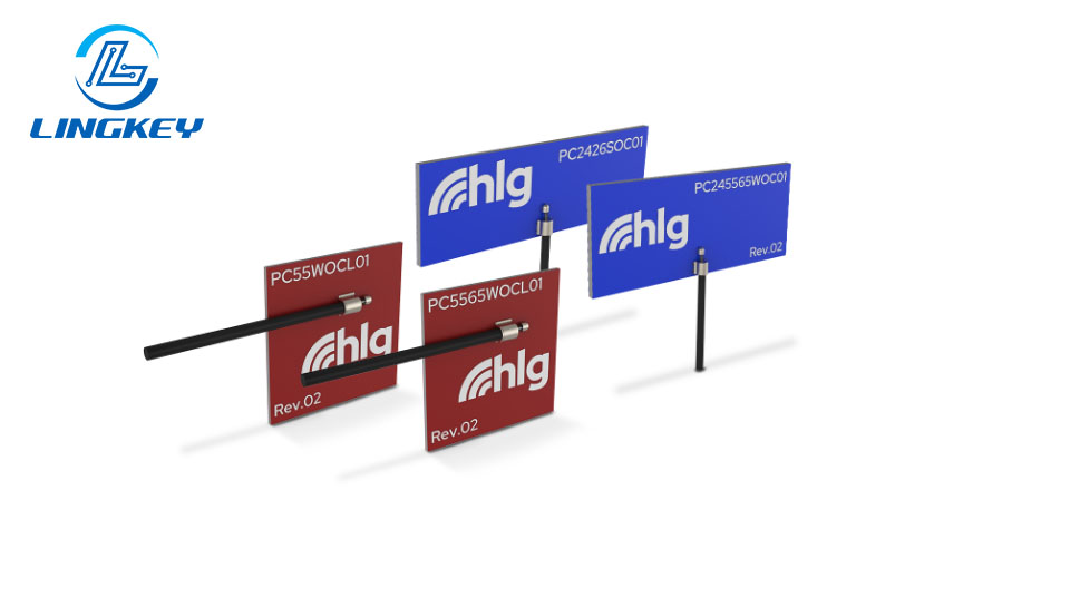
PCB Antenna vs Chip Antenna
When deciding between a PCB antenna and a chip antenna (which is a pre-manufactured component), designers should weigh several factors:
Factor | PCB Antenna | Chip Antenna (Pre-manufactured) |
Cost | Lowest (printed on PCB) | Higher (component cost) |
Size Flexibility | Fully customizable; fits size and shape of board | Fixed dimensions |
RF Performance | High if careful design is applied | Consistent, less sensitive to layout |
Tuning Capability | Excellent; can adjust during PCB layout | Limited; relies on matching network |
Placement | Integrated with RF circuitry | Can be located for ideal placement |
Assembly | No extra parts; reduces steps | Adds a step to assembly |
Application | Good for volume, integrated systems | Good for products with space constraints |
Flexible antennas represent another option they are compatible with products that must be bendable (wearable, foldable electronics) yet necessitate extra processing steps.
Applications and Case Studies
Wi-Fi Applications
A wi-fi antenna(sometimes a patched or slotted monopole)is usually present in wireless routers and embedded devices. The design, including layout and matching, affects coverage and throughput of the devices. A typical example is the slot antenna for dual band applications.
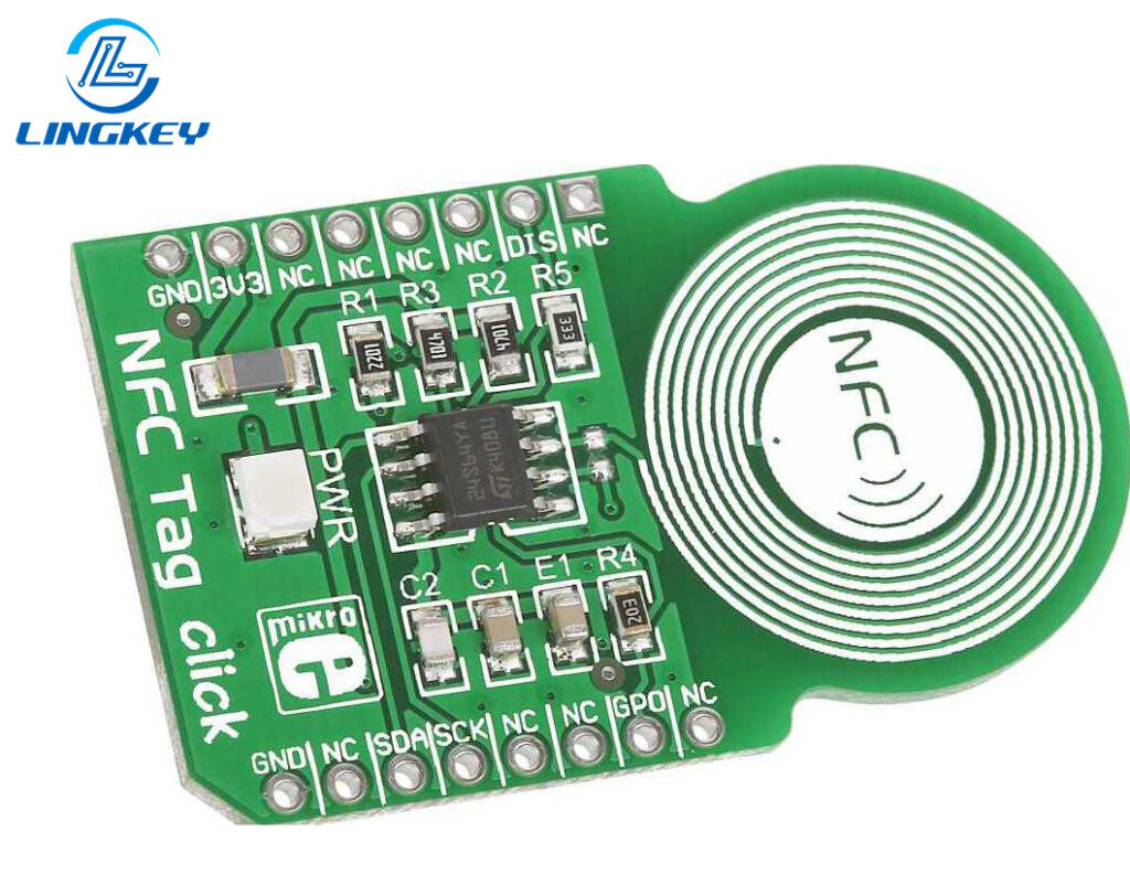
NFC Applications
For NFC, a loop or meandered antenna printed on a single side of the PCB is essential. The antenna needs to be tuned at 13.56 MHz, which is widely employed in RFID for access cards and mobile payment gadgets, the antenna is sensitive to magnetic field and metal item in proximity.
RFID and IoT Devices
Slot and dipole antennas are popular in RFID systems. For the IoT a custom monopole or dipole antenna is provided ensuring reliable communication to the gateways. Antenna placement and PCB material selection are critical when designing a PCB for these markets because of low power and high integration.

Future Trends in PCB Antenna Technology
- Multiband/Compact Solutions:Multi-standard devices need antennas for use on several bands, which can be done by means of an advanced rf design and new al-based pcb material science.
- Flexible and 3D Antenna Structures:More devices are now employing flexible antennas, which can expanded using modern pcb fabrication methods.
- Automation:Careful design and optimization using AI-assisted simulation is being embedded into commercial RF tools, greatly speeding up the antenna design cycle.
Frequently Asked Questions
Can changing PCB material affect antenna performance?
Can a PCB antenna replace a separate antenna in all cases?
What design considerations are most important for optimal signal integrity?
Are PCB antennas suitable for MIMO Wi-Fi or LTE?
Why Choose LingKey PCB Antenna Solutions?
- Extensive expertise in designing a PCBwith integrated radiating elements for wireless protocols.
- Free antenna consultancy for optimal RF performance and seamless schematic-to-prototype assistance.
- Experience with various PCBmaterials, including high-frequency substrates for demanding communication systems.
- Rapid prototyping and in-house PCB fabricationto validate complex or unconventional antenna designs.
- Mass production capabilities to deliver consistent quality, whether you need one side of the PCB or dual-sided solutions.
Good knowledge of PCB antenna layouts and RF-aware fabrication processes from LingKey’s production expertise with high frequency and mixed material PCB platforms.
Conclusion
As the technology advances towards miniaturization, intelligent and integrated communication system, the application of PCB antenna has become the best choice for getting rid of the bulky, isolated antennas. Given that there are so many different types of antennas (monopole, dipole, patch, slot, flexible, and so on) and now with proper pcb material, layout and antenna design techniques the combination is limitless. With ingenuity, simulation, and testing, high performance and reliability and cost savings can be achieved, enabling the next generation of wireless innovation.
Validation of designs and volume manufacturing Experienced PCB vendors like LingKey are the key enablers in taking PCB antenna designs through to robust, mass produced wireless solutions.
")
")


")
")
")


