Ultimate Guide to PCB Repair & Rework
Table of Contents
ToggleIntroduction
The printed circuit board (PCB) is the base for almost all modern electronic gadgets, functioning as the backbone that facilitates electrical signals flowing among the components on the circuit board. Their importance plays a part in everything from smartphones and power supplies to industrial control systems. Knowing how to fix PCBs and performing printed circuit board repair is a useful skill for anyone who works with electronics, whether you’re maintaining equipment you have more than a decade of experience with, or are confronting a malfunctioning circuit board for the first time.
This is not only about the best practice of reliable PCB board repair, but also about the common failure mode of circuit board, best repair tools and techniques as well as simple but effective step of repairing circuit board that help avoid throwing good board to waste because of some broken pads or traces. Well-drafted PCB repair procedure for high-end board results in extending the life of good PCB assembly and it saves the need to have new board in place when localized repair is sufficient.
Understanding PCB Structures & Common Failure Modes
PCB Structure Essentials
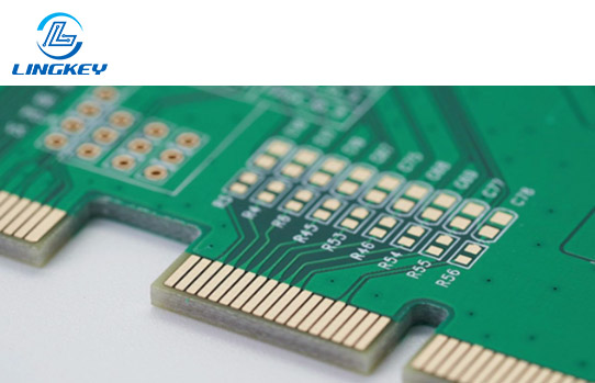
A pcb board consists of multiple layers and features that are engineered to allow the assembling and operating of many electronic parts. The key factors to reliable PCB design and manufacture are:
Layer/Feature | Purpose |
FR-4 Substrate | Foundation for pcbs function; provides rigidity and insulation |
Copper Traces | Pathways transmitting signals and power; part of every PCB assembly process |
Vias | Small, plated holes connecting board surfaces and inner layers |
Solder Mask | Protects copper and solder joints; prevents accidental shorts |
Silkscreen | Component labeling; eases board assembly and maintenance |
A good quality PCB is designed and the design process is followed so that it can work for years and years with durable and efficient working.
Common Types of PCB Failure
Knowing what causes a circuit board failure is the key to its repair:
- Physical Damage to Circuit Boards:Astigmatism in objective due to mishandling, shock, or excessive tube stress.
- Component Failure:Overheated, aged, or power surged electronic elements may be destroyed, causing the board or nearby components to malfunction.
- Trace Damage:Breaks, burns, or corrosion interrupt copper traces, often invisible to the naked eye.
- Soldering Errors:Bad solder joints or too much heat can cause an open or intermittent connection, or overheating in the repair area.
- Poor PCB Design:Insufficient trace width, lack of thermal reliefs, or incorrect routing can cause circuit boards to fail earlier.
- Environmental Factors:Moisture, contaminants and thermal cycling lead to corrosion and deterioration of circuit elements.
- High-Temperature Exposure:Repeated hot/cold cycles or nearby short circuits melt solder, delaminate boards, or lift pads.
- Electrostatic Discharge (ESD):Static surges damage sensitive components on the circuit board.
With these typical failures, you can diagnose and fix causes which bring the entire PCB back to life.
Tools, Materials & Safety for PCB Repair
Professional pcb repair needs the right repair equipment and appropriate safety precautions to avoid damage to the circuit board.
Essential Tools and Materials:
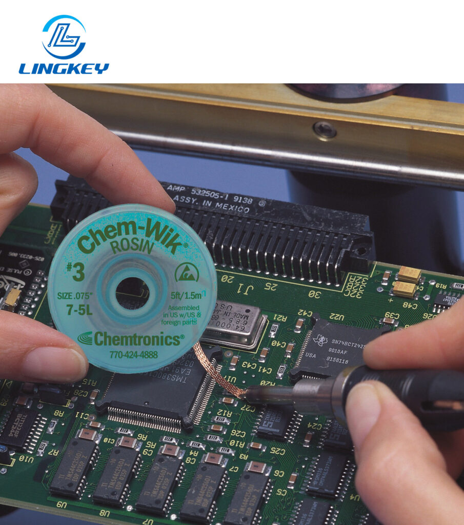
- Soldering Iron:For removing and installing components and making strong solder joints. Use a temperature-controlled unit for best results.
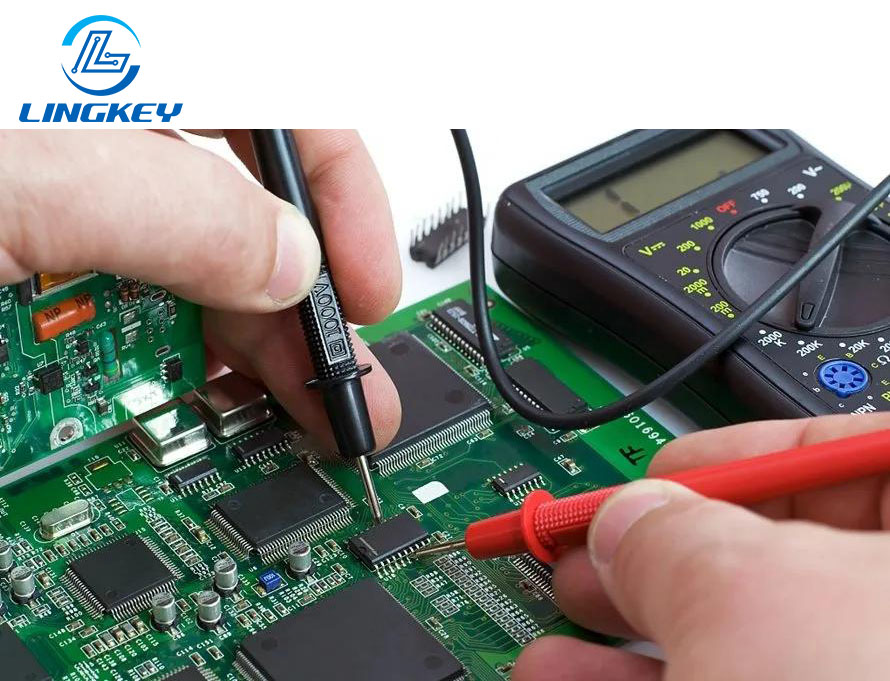
- Digital Multimeter:For continuity checks, diagnosing faults, and confirming proper function.
- Solder Wick and Solder Sucker:Wick removes unwanted solder; the spring-loaded vacuum draws melted solder through the hole in the middle, freeing pins or pads.
- Hot Air/Heat Gun:Used to melt all the solder on multi-pin devices; essential for SMD/PTH rework.
- Magnifier or Microscope:Reveals micro-cracks and defects not visible to the naked eye.
- Isopropyl Alcohol:For cleaning burnt flux, corrosion, and debris from the board surface and repair area.
- Copper Foil Tape/Jumper Wire:Repairs damaged copper traces, restoring connectivity and signal integrity.
- Conductive Ink:For intricate trace or pad repairs.
- Epoxy Resin:Strengthens lifted pads and anchors wire repairs.
- Antistatic Wrist Strap:Prevents ESD from damaging sensitive PCB components.
Safety First:
- Always fully discharge boards before starting repair.
- Handle all chemicals, including alcohol and flux, with care.
- Maintain ESD protection—static can cause circuit boards to fail even if repair is correct.
- Protect nearby components on the board during soldering or hot air work.
Diagnosing PCB Damage and Troubleshooting
A correct diagnosis is the key to successful pcb board repair. Follow these step by step systematic procedures to detect circuit board damage:
- Visual Inspection:Under a magnifying lens, inspect for burnt spots, broken traces, or discolored solder joints that would make the board fail.
- Continuity Testing:Check for opens or shorts with a multimeter, comparing to the schematics if you have them.
- Thermal Checks:A heat gun or thermal camera can reveal overheating components or traces.
- Defects and Repair History:Record symptoms and prior repairs for a complete guide to troubleshooting.
- Check for Faulty Components:Detect and mark any damaged parts or defective connectors which must be taken out or substituted.
Knowing the exact cause of failure, whether a single component or a group of circuit elements is at fault, contributes to a successful repair.
Step-by-Step Guide: How to Repair PCBs
Trace Repair
One of the more common ways of fixing a circuit board is the repairing of broken traces:
- Identify the Damage:Clean with isopropyl alcohol. Use a magnifying glass to find cracks that can’t be seen with the naked eye.
- Expose the Trace:Carefully scrape away the solder mask with a craft knife, but don’t make the center hole too big and damage the surrounding copper.
- Bridge the Gap:Use copper foil tape, jumper wire, or conductive ink to cover the distance in the gap. Solder it tight to the electrical connection.
- Confirm:Use a multimeter for continuity.
- Protect:Apply solder mask, conformal coat, or pot with epoxy for environmental protection and mechanical support.
Pad and Via Repair
The soldering mistakes and rework heat and mechanical strain can be the worst for the world for pads and vias.
- Clean the Repair Area:Remove debris and old solder.
- Anchor a New Pad:Craft a pad from copper foil, glue it down with epoxy, and solder as needed.
- Via Repair:Pass a wire through the hole; secure and solder each end to reestablish connection across inner layers of the board.
Component Replacement
When a damaged component or defect is the root cause:
- Desolder and Remove:Apply heat with a soldering iron and the solder wick or a hot air tool and when the solder melts, apply a spring vacuum to suck the molten solder.
- Install the Replacement:Tlid the new component, with polarity and orientation, and then inspect the connections for cold or bridged joints. Test: Power up the board and verify functionality across all repaired sections.
Gold Finger and Hole Repair
Repairing gold fingers and damaged holes requires detailed work:
- Gold Finger:Clean, then apply gold conductive ink or send for professional re-plating if needed.
- Repair the Hole:For a bad via or pad, wire it, reinforce with epoxy, and solder on both sides to restore the trace.
Best Practices and Tips for Reliable PCB Repairs
To ensure lasting results and maintain signal integrity:
- Work Static-Free:Use ESD protection at all times—even a small discharge can cause circuit board failure.
- Match Materials:For the best circuit board performance, the trace width, copper thickness and layout should always be the same as those of the original pcb design.
- Control Heat:Avoid overheating, which can damage the circuit board or cause further failures.
- Work Delicately Around Nearby Components:Too much pressure or heat can damage parts of the circuit board that are not involved in the repair.
- Clean Thoroughly:Remove all flux and debris after every step.
- Document Everything:Maintain logs for defects and repair history.
Repair vs. Replacement: Cost & Benefit Analysis
Occasionally the choice to fix circuit board errors or to swap out a board is not clear-cut.Here is a practical comparison:
Factor | Repair PCB Board | Replace It With a New Board |
Cost | Often much lower, especially for localized repairs or damages | Higher, includes material, shipping, and assembly costs |
Speed | Immediate if tools and expertise are available | Can be delayed by sourcing, shipping, and PCB assembly process |
Availability | Local repairs possible even for discontinued designs | May not be possible for obsolete or custom boards |
Sustainability | Reduces electronic waste, maximizes use of electronic equipment | Completely new manufacturing increases waste |
Skill Required | Requires experience and care, especially for multi-layer or complex repairs | Minimal technical skill, but may involve final configuration |
Reliability | Excellent if completed using best practices for reliable repairs and tested | Factory new reliability, but other system issues may persist |
Board Complexity | Possible to repair most single/double layer PCBs; multi-layer or inner layer damage may be prohibitive | All types possible, assuming design specs are available |
PCB Repair Kits, Tools & Service Recommendations
When you’re gearing up for PCB board repair or pcb rework, make sure you buy tried and tested dependable gear. The following is a comparison of the recommended kits and essential tools for repairs:
Kit/Tool | Contents | Best Use Cases | Where to Buy |
iFixit Pro Tech Toolkit | Precision screwdrivers, ESD strap, solder iron | General PCB and electronics repair | iFixit, Amazon |
Chemtronics CircuitWorks Repair Kit | Conductive ink, copper tape, flux pens | Trace & pad repair, SMD work | Major distributors |
MG Chemicals 8329TF Epoxy | Thermally-conductive epoxy | Pad/via repair, mechanical reinforcement | Digi-Key, Amazon |
Hakko FX-888D Soldering Station | Professional soldering iron, temp control | Reliable solder joints, rework | Hakko dealers |
Quick 861DW Hot Air Rework Station | Hot air gun, temperature controls | SMD work, reflow soldering | Electronics shops |
Kaisi Multimeter + Toolkit | Multimeter, solder wick, tweezers | Troubleshooting and basic repair | AliExpress, eBay |
For the professional PCB design, fabrication and assembly services, an experienced one stop solution supplier like LingKey can support for your custom PCB requirements, and help with manufacturability repair or rework on high cost and complicated assemblies.
Frequently Asked Questions About PCB Repair
What are the common causes of circuit board failure?
Can I repair a faulty circuit board at home?
How do I know if a damaged PCB is repairable?
Are repaired boards as good as new?
Should I attempt to repair a PCB if I have no experience?
Conclusion
Mastery of pcb board repair is a realistic, cost-effective and green way to prolong the life of your electronic equipment. Whether you’re tracing damage to circuit components, doing printed circuit board repair on a mission-critical power supply, or doing a complete PCB rework, the processes outlined in this authoritative guide ensure reliable, safe and high-quality results. The bottom line: If you understand board makeup, what fails (generally), and the need for thorough diagnosis and proper repair area methodologies, you can breathe new life into circuit boards and bring full function back to devices that would otherwise be sent to the landfill.
")
")


")
")
")


