What are Tented Vias? A Comprehensive Guide
Table of Contents
ToggleIntroduction to Tented Vias in PCB
In the fast developing PCB field, all new PCB designers have to deal with the row of printer circuit board layouts in the rows, of copper connections, and the protective measures that enable cost effectiveness and function reliability. In this regard, vias are of great importance as they connect traces on the different layers of a PCB, enabling the creation of small, large, and complex high-density PCB layouts. However, just drilling out and exposing vias can create contamination and assembly issues. This is where the process of tenting vias in pcb assembly becomes so important.
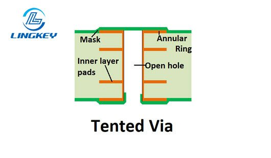
What is a Tented Via?
A via that’s tented on one side may still permit limited access for probing; a via tented on the bottom side but open on the top is an example of one-sided tenting. Conversely, when both sides are covered, the via is“fully tented.” In context, tented vias in pcb design means the engineer has decided to cover (tent) all or some vias to satisfy certain protection requirements or pcb design rules.
Tenting via is the process to cover via and via barrel (the inside of a via is a copper-plated tube) with a layer of solder mask, normally done in the PCB manufactory. Both standard through-hole vias and small vias can be tented with conventional solder mask or with advanced dry films. Tenting helps to prevent solder wicking, contamination or accidental bridging under PCBA process.
Types of Vias and Tenting Methods
Types of Vias in PCBs
Inside any normal PCB, you’ll find a variety of vias:
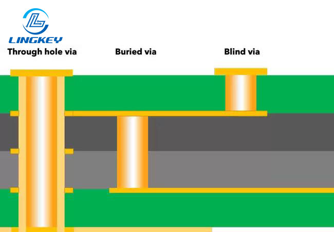
- Standard through-hole vias: Vias are copper-platedand penetrate the full PCB thickness.
- Blind vias: Connect an outer layer to an inner layer without passing through the entire board.
- Buried vias: Only connect inner layers, never reaching the top or bottom surfaces.
- Microvias: Extremely small vias, crucial for high-frequency PCBdesigns and miniaturized applications.
- Via in pad: Pads that are conformal over a via; typically filled with solder or epoxy, then plated – a process used for high BGA and micro-BGA assembly.
Types of Tented Vias
- Fully tented vias: The solder mask covers both the top of the via and the bottom, sealing off both ends.
- Partially tented vias/tented on one side: Only one opening of the via is masked, either on the top or the bottom.
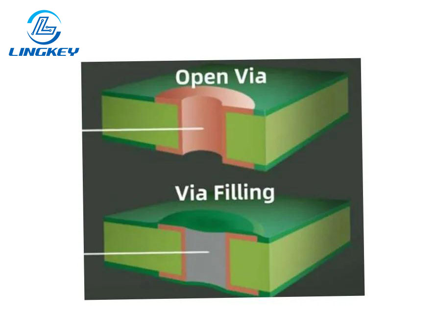
- Untented vias: Exposed, with no solder mask coverage. An untented viais prone to contamination and solder bridge risks.
- Tenting vs. Untented vs. Plugged/Filled: See comparison table below.
Aspect | Tented Via | Untented Via | Plugged/Filled Via |
Protection from Solder | Yes | No | Yes |
Prevent Solder Wicking | Strong | No | Highest |
Electrical Test Access | Limited (full tent) | Full | None (infilled) |
Cost | Low | Lowest | High |
Methods for Tenting
- Tenting process: Application of a solder mask and dry filmover the via, followed by exposure, curing, and inspection.
- Filling vs. covering the via: Advanced designs like via in padrequire the via to be filled with solder or epoxy before overlaying with mask for planarity.
- Hybrid approaches: In harsh environments, hybrid via treatmentsblend tenting with plugging or conductive fillers for extra durability.
Why Are Tented Vias Used in PCBs?
The benefits of tented vias are substantial:
- Prevents solder wickingduring reflow, essential in dense PCB layouts where vias near pads could otherwise wick solder away from the component.
- Contamination protection: The mask can crackif mishandled or incorrectly cured, but when properly processed, it reliably seals contaminants inside the via barrel.
- Aesthetic improvement: Tenting creates a consistent board finish, hiding the metallic via barrelsand supporting branding in consumer electronics.
- Durability and reliability: Sealing the via prevents corrosion, dust ingress and moisture, which is essential for high frequency PCBs as well as automotive and industrial applications.
Advantages and Disadvantages of Tented Vias
Key Advantages:
- Contaminant Exclusion: Blocks solder and dust from getting inside the via barrel.
- Enhanced PCB Reliability: Reduces short circuit and EMI risks, especially with vias alongpower and signal routes.
- Cost-Effective: Easier and cheaper than plugging or filling.
- Prevents Solder Wicking: Protects component joints by stopping solder from disappearing inside the via.
Key Disadvantages:
- Access Issues: Full tenting restricts electrical testing
- Potential for Incomplete Coverage: Large or misaligned vias may remain partly exposed, no longer functional as a “tented” structure.
- Mask Concerns: Solder mask can causeproblems if improperly applied or if the mask can crack due to mechanical or thermal stress.
- PCB Assembly Constraints: Tented vias are platedand then masked—thicker plating or large diameters make it hard to fully seal the via.
Key Parameters and Specifications for Tented Vias
- Via Diameter: Small vias(ideally <0.3mm) are best suited for tenting.
- Aspect Ratio: The pcb design rulesmay specify a max aspect ratio (board thickness / via diameter) to ensure dependable tenting.
- Solder Mask Layer: The thickness, type (LPI or dry film), and process control of this layer are critical to longevity.
- Positioning: Placing viasnear pads requires extra attention to avoid bridging.
- Tented on the Bottom Side vs. Top: Only select “tented on the bottom side” if testing or repair from the top is required, but this does expose the via to some contaminants.
Design Considerations and Best Practices for Via Tenting
- Include tenting in the PCB fabrication files: Specify clearly which vias to tent (or not) for your PCB assembly
- Consider via location: Avoid placing tented vias right next to sensitive high-frequencytraces—unwanted parasitic capacitance or impedance changes may arise.
- Follow industry standards: Guidelines such as IPC-4761 Type I(tenting via with dry film solder mask) establish best practices.
- Use solder mask dams: To avoid shorts between pads and adjacent vias, employ solder mask dams where possible for clarity and safety.
Every PCB is different: Guide your tenting strategy for the product environment, PCB design rules, and your manufacturing partner’s advice.
Tented Vias vs Plugged, Filled, and Untented Vias
Tented vs. Untented Vias
Tented Vias | Untented Vias | |
Solder Protection | Excellent | None |
Contamination | Yes, protection from above/below | None |
Rework/Test | Difficult (full tent); ok (one-sided) | Easy |
Cost | Low | Lowest |
Applications | Mass production, consumer, light industry | Prototyping, test, short-run |
Plugged and Filled Vias
Plugged/Filled: When it come to reliability and planarity (consider via in pad or BGA footprints), filled vias guarantee no voids or exposure. For the high-grade reliability PCB designers for severe environment, this process is also the popular one in spite of the higher cost.
Tented Via Manufacturing and Assembly Process
A typical tenting process in PCB fabrication includes:
- Drilling(vias are used to link layers),
- Copper Plating(vias are copper-plated by default to create electrical connectivity),
- Solder Mask Application(dry film or LPI, covering the vias),
- Curing
- Inspection(often with AOI— Automated Optical Inspection—for thorough defect detection).
- Final Assembly: After curing, the PCB assemblyprocess continues. The tented vias are now shielded from solder, flux, and debris during component placement and reflow.
It’s important to remember that tented vias are plated just like any other via before the solder mask is applied. Whether you choose to tent only some vias (perhaps those near BGA pads or traces dealing with critical signals) or tent all vias in certain regions, the tenting must be specified in your pcb fabrication notes to prevent errors in production.
Applications of Tented Vias
Tented vias are incredibly versatile across PCB sectors:
- Consumer Electronics: Smartphones, tablets and the like use tenting to prevent solder wicking and contamination, shielding the functionality of the device as well as maintaining the aesthetic expectation of these products.
- Automotive Electronics:ECUs and ADAS employ tented vias to provide moderate protection from the environment and to improve the life of the
- LED Lighting: Tented vias prevent electrical shorts and contamination in LED drivers, leading to higher PCB reliability for long-life applications.
- Communication and High-Frequency PCB: In high frequency router, rf module, and telecom hardware pcb designs, sealing is used to ensure signal integrity by keeping out contaminants and by keeping out spurious conductive paths.
- Industrial Equipment: Automation controllers and sensor modules employ tented vias to resist factory moisture, dust, and sporadic abuse.
Challenges in Tented Via Manufacturing
While tenting is a straightforward process, several challenges persist:
- Coverage Uniformity: Achieving full coverage is difficult with larger vias or when high density layout forces a number of vias to be located in the same area. Poor coverage may result in the exposure of the via or in the entrapment of contaminants.
- Cracking and Adhesion: The solder mask may cause reliability issues if mishandled. Mask can fracture under thermal cycling or PCB bending repeatedly, particularly for PCBs subjected to vibration or temperature variations.
- Void Formation and Outgassing: Bubbles within the tent may inflate during the reflow cycle, compromising the integrity of the tented area and potentially influencing nearby vias in proximity to heat sources.
- PCB Industry Variation: Reliable tenting capability is a function of the technology level of the vendor and their experience with high-end solder mask and dry film materials and equipment. Not all pcb shops do assured full tenting for large-diameter vias.
Impact of Tented Vias on PCB Performance and Reliability
Tented vias contribute significantly to overall PCB reliability:
- Signal Integrity: In the RF and high-speed PCB design, tented vias reduce the possibility of stray currents and keep the impedance environment controlled, which is always important for signal speed at gigahertz or above.
- Durability: Preventing the ingress of contaminants in the via barrel can reduce latent failures from corrosion or dendritic growth.
- Moisture and EMI Protection: In fact, for outdoor, automotive or mission critical electronics, tented vias provide a straightforward yet reliable seal against moisture-caused failures and EMI.
- Assembly Yield: Avoiding solder wicking provides for a fully soldered and robust component lead, which reduces the likelihood of failure in field and rates of repair following assembly.
Cost Implications and Trade-Offs
Although via tenting in PCB assembly is among the most economical means of via protection, there are some trade-offs to be considered:
- Cost Advantage: Tented or one- side tented vias do not require any special material other than the normal solder mask, thus it is very scalable for the mass production.
- Testability: If full electrical probe access is required, consider untented viasor tented on one side approaches for balance.
- Critical Circuits and Harsh Environments: In the maximum hardness environments (aerospace, military), plugged or filled by methods—are more expensive, but worth the investment.
Future Trends in Via Tenting
- Increasing Use of Automated Inspection: With boards getting denser, AOI and x-ray inspection are more common to make sure of the quality of tenting.
- New Solder Mask Materials: Improved photo-imageable solder masks provide greater flexibility and fewer possibility of cracking of the mask with aging.
- Tenting Plus Plugging: In the most critical board areas, some PCB designers now combine tenting with partial fill or conductive paste and gain both low cost and high reliability.
Case Studies & Real-World Examples
Case Study: Telecommunication Router PCBs
A manufacturer experienced solder wicking in critical signal vias while assembling PCBs. By mandating that critical vias be tented (and by employing solder mask dams around vias from neighboring pads), solder wicking was drastically reduced, assembly yields improved, and high frequency signal attenuation was lessened.
Case Study: Automotive Power Modules
In the initial designs, vias were not tented or only tented on one side and would corrode when subjected to condensation in engine bays. Transitioning to fully tented vias with enhanced solder mask and dry film materials as well as selective use of filled vias in the highest risk areas prolonged product life by 40%.
Tips for Ordering Tented Vias and Working with PCB Manufacturers
- Specifically identify via tenting requirementsin your design files and notes—e.g., “May need to be tented all vias except test points.”
- Discuss with your manufacturerthe available options for small vias, one-sided tenting, and requirements for a specific tenting process.
- Clarify if via in pador other special via structures (such as blind vias or buried vias) require unique tenting or filling instructions.
- Verify fabrication capabilitiesfor both typical and advanced solder mask materials, especially for dense boards (high-frequency PCB, microelectronics, etc.).
- Request sample cross-sectionsand optical inspection reports if your design depends on tenting integrity for reliability.
- Stay updatedby reading recent articles on PCB design, as technology and best practices are continuously evolving in the PCB world.
Frequently Asked Questions about Tented Vias in PCB
What does “tenting a via” mean in PCB design?
Are tented vias plated before masking?
Is it better to have tented or untented vias?
Do tented vias work with buried or blind vias?
Will tented vias affect the assembly process?
Conclusion: Should You Use Tented Vias in Your PCB Design?
In general, tented vias for PCB design have become a standard methodology for PCB designers who wish to minimize the risk of contamination, eliminate solder wicking, and enhance reliability and visual uniformity. Although via tenting is not a panacea – bad tenting can do the same or even more harm to buried or blind vias – it is still a well-established, cost effective and scalable technique when used with good design rules and manufacturing best practices. As a result of repair, testing or environmental considerations, product developers may choose to one-side tent, leave specific test points untented, or combine tenting with plugging or filling for critical applications.
Consistent via tenting is a matter of communication, good PCB design rules, and working closely with your fab house. Through the entire process of PCB manufacturability and assembly yield, LingKey considers via tenting as a natural way. The application of accurate solder mask control, proven process capability and engineering support during fabrication and assembly, LingKey is able to provide assurance that tented via will perform as intended, protecting critical circuit, enhancing assembly robustness, and supporting long term product reliability in a broad range of applications.
")
")


")
")
")


