What is a PCB? Complete Guide to Printed Circuit Boards, Types, Structure, Applications, and Manufacturing
When it comes to modern electronics, the PCB is the backbone. And they are at the core of virtually every electronic component you use every day — from your phone to aerospace gear, and everything in between like industrial control systems. This comprehensive guide will explain what a PCB is, the design process, major types and structures, how PCBs are used and made and the significance of PCBs for the current technology.
Table of Contents
ToggleIntroduction to PCBs
What is a Printed Circuit Board?
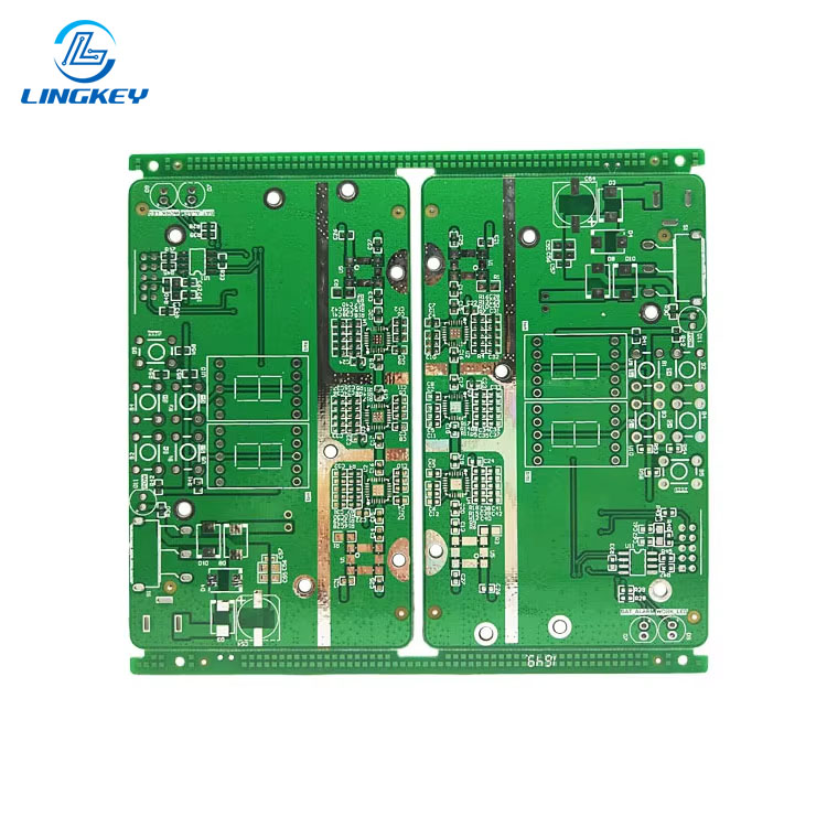
A PCB is a board material which mechanically supports and electrically connects electronic components using conductive pathways, or traces, that are etched from copper sheets laminated onto a non-conductive substrate. Now, printed circuit board and circuit board assembly (PCA/PCB Assembly) replaces the bulky manual wiring to realize high-density, high-efficiency circuits.
LingKey is a professional multilayer, HDI, rigid-flex, high-frequency, high-reliability PCB manufacturer, serving a wide range of industries such as consumer electronics, automotive and aerospace.
How Do PCBs Work?
PCB, at its core, is a medium to route traces between components like thin conductive copper lines or paths, which defines an exact pattern to make electrical connections between components. These traces dimension a network that can be used to send electric signals of power, data, or control from one side of the board to the other.
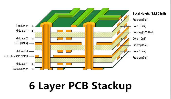
PCB Layers and Connectivity
Most boards are multi-layer, designed with ECAD (Electronic Computer Aided Design) tools. The stack-up design is important, as it affects impedance control, signal integrity and reliability. This PCB stack-up can be single-sided or double-sided, and for more complex devices, have multiple (even dozens) of layers.
Layer | Purpose |
Substrate | The non-conductive base material (FR-4, polyimide in flex boards) |
Copper Traces | Conductive paths that create electrical connections |
Solder Mask | Protects copper and isolates traces |
Silkscreen | For labeling, part IDs, and design review marks |
Copper Planes | Used for power distribution and ground return; impedance control |
Make PCBs Work for You
- Ensure proper design review and verificationbefore manufacturing.
- Use pcb design toolsand design software to simulate and optimize the design.
- Electronic computer-aided design (ECAD) tools facilitate the entire design workflow.
Types of PCBs
What a PCB looks like and does depends on it’s tailored design and purpose. So when you are designing, you need to know what type of stack-up you want for your application.
Type | Description / Use Cases |
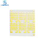
Single-sided | Used to build low-cost devices like calculators; conductive layer and components are soldered on one side only. |
Double-sided | Traces and pads/both sides; used in applications needing moderate complexity. |
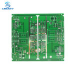
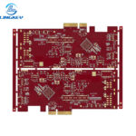
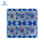
Multilayer | Stack of 3+ layers; vital for mobile, computing, and advanced driver-assistance systems. |
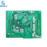
Rigid PCB | Most common; used for everything from smartphones to TVs and industrial controls. |
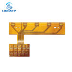
Flexible | Thin polyimide substrate; ideal for wearables and cameras. |
Rigid-Flex | Combines rigid and flexible for 3D shapes in aerospace or medical. |
High-Frequency/RF | For radar, wireless, and telecom, with tight tolerance and impedance control. |
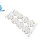
Aluminum/Ceramic | Handles high temps in LEDs or power electronics |
Key Point:
PCBs are used in applications ranging from simple toys (single-sided or double-sided) to multi-layer rigid boards for servers, and flexible/ridgid-flex for complex wearables and industrial applications.
Structure of a Printed Circuit Board
The conformation of a typical PCB is the outcome of subtle mechanical and electrical interactions.
- Substrate:The insulating, non-conductive foundation (flat board), usually FR-4 for rigid PCB design.
- Copper Traces & Pads:Patterned using ECAD tools; these connect the components and form all electrical signals
- Solder Mask:Protects traces and stops solder bridges—often green, but available in many colors.
- Silkscreen:Marks, logos, and part numbers for easy design review and electronic assembly.
- Vias and Holes:Connect layers and enable surface mount technology assembly or through-hole components.
- Connector: Used to hold or join the PCB to other devices or signal paths.
Layer | Function |
Substrate | Mechanical support (flat board) |
Conductive Layer | Circuit routing (traces and pads) |
Solder Mask | Electrical insulation, prevents short circuits |
Silkscreen | Markings for ID, orientation, circuit diagrams |
The stack-up and number of layers are customized for the required shape and function. Layers are laminated under heat/pressure, resulting in a rigid end product.
Applications of PCBs
Almost every electronic product utilises PCBs. Boards are employed as the physical means to connect electronic components, to power them and to handle the signals.
Most Common and Critical Applications
- Consumer Devices:Everything from smartphones and tablets to TVs and gaming consoles
- Automotive/ADAS:Engine controllers, infotainment, advanced driver-assistance systems
- Medical Devices:Imaging, ECG, and portable monitors, where impedance control and reliability are vital
- Industrial Applications:Robotics, PLCs, and factory control systems, where rugged, rigid PCBs excel
- Aerospace/Defense:Avionics, communications, and radar with strict requirements on stacking, layout, and heat control
- IoT and Edge Devices:Sensors, trackers, and lightweight controllers
How Are PCBs Manufactured?
The PCB layout turns the idea of the circuit diagrams into a design that can be manufactured as a physical object. It starts with the use of electronic computer-aided design, continues with design review, and ends with accurate fabrication and assembly.
LingKey has the high-level ability in PCB manufacturing and SMT assembly. We support prototypes to volume production with stringent IPC-Class quality assurance and full traceability.
The Design Workflow to Manufacturing
- Design & Schematic Capture:Draw circuits, define electrical signals using ECAD/EDA pcb design software (software is used widely such as Altium, Eagle, KiCAD).
- PCB Layout:Arrange components and route traces between components. Stack-up is defined for impedance control, power, and signal layer management.
- Design Review and Verification:Confirm with simulation and DRC tools.
- Preparing for Manufacturing:Generate Gerber files, define pcb stack-up, review all parameters.
- Fabrication:
- Layers are laminatedand patterned via etching.
- Viasand holes drilled.
- Surface finish, solder maskand silkscreen applied.
- Assembly:
- Components are solderedusing surface mount technology or through-hole.
- Automated machines for volume; X-ray, AOI, and electrical testing for quality.
- Final Review and Testing:
- Inspection ensures the board is readyfor deployment.
Step | Details & Tools | Purpose |
Schematic Capture & Design | Schematics designed using ECAD software (Altium, KiCAD, Eagle, and so on) | Specify all the electrical signals and connections among components. |
PCB Layout | Using PCB design software for board outline, stack-up, and placement | Place and route traces to make the connection between the components as needed. |
Design Review & Verification | Simulations, DRC (Design Rule Check) & signal analysis tools | Ensure functionality, impedance control, manufacturability |
Preparing for Manufacturing | Generate Gerber, drill, and BOM files | Specify details needed for fabrication and assembly |
Fabrication | Copper etching, layers laminated, drilling, surface finish, mask & silkscreen | Create the physical board according to the entire design |
Assembly | Components are soldered using SMT or through-hole techniques | Turn the bare PCB into a functional electronic assembly |
Inspection & Testing | Visual, electrical, AOI, and X-ray inspections | Quality control and assurance before deploying the board |
Benefits of Using PCBs
PCBs provide a plethora of benefits that result in their widespread application in various fields :
- Scalability & Consistency:Automated fabrication and assembly ensure every unit is identical, supporting mass production.
- Form and Function:Multilayer and stack-up design allow for incredible miniaturization while meeting performance requirements.
- Reliability:Boards provide secure, repeatable electrical connections, minimizing faults due to manual wiring errors.
- Efficient Troubleshooting:Systematic design and clear silkscreening support efficient design review and field maintenance.
- Cost Effectiveness:Once the design process is optimized, large-scale fabrication keeps unit costs low, particularly for rigid PCB designs and common industrial applications.
- Signal Control:Advanced PCB using impedance control and proper layout enables high-speed signal transmission critical for everything from smartphones to industrial robots.
Key Factors When Choosing or Designing a PCB
When developing or specifying a PCB, several factors should guide your choices:
Factor | Why it Matters |
Intended Application | Dictates stack-up design, substrate type, and environmental requirements |
Electrical Requirements | Impedance control is crucial in high-speed and RF designs |
Mechanical Constraints | Consider board size, mounting, and whether you need a rigid PCB or a flex PCB |
Thermal Management | Vital for power electronics and LEDs, dictating copper thickness and stackup |
Compliance & Safety | Must meet industry standards for reliability and electronic assembly |
Design Workflow | Selecting robust PCB design tools and ensuring design review steps |
Cost & Volume | Influences whether to use a single-sided, double-sided, or multilayer design |
Common Issues and Troubleshooting for PCBs
Even with a flawless design process and advanced manufacturing, issues may arise:
Frequent Issues
- Poor Solder Joints:Result from improper SMT placement or wrong temperature profiles during assembly.
- Delamination:Layers not properly laminated can peel apart, often due to excessive heat or humidity.
- Trace Breaks or Shorts:Caused by over-etching, accidental bridging, or poor design practices.
- EMI Problems: Inadequate ground planes or poor routing can result in interference, particularly in boards used for RF.
Troubleshooting Steps
- Use an ECAD viewerto examine the design alongside the physical board during review.
- Check all connectors and component placement against the circuit diagrams.
- Use a multimeter or flying probe tester to test conductance and find open or short circuits.
- Verify surface mount and through-hole solder connections with magnification or AOI systems.
Innovations and Future Trends in PCB Technology
PCBs are critical to innovation should now be clear.New trends are evident, showing electronics manufacturers and end users are evolving and their needs are changing.
- HDI and Miniaturization:More layers and advanced stack-up design enable smaller, more powerful devices.
- Smart, Embedded Components:Boards now embed passives and even entire chips within the laminate.
- 3D Printing and Additive Manufacturing:The future may allow design into a physical PCB in hours, not days.
- Green Boards:Materials and processes that promote recycling and reduce hazardous waste are now in demand.
- Integrated Design Software:Cloud-based ECAD and design tools enable real-time collaboration, speeding up the design workflow.
Frequently Asked Questions About PCBs
What is the difference between a PCB and PCBA?
How do I start the design process?
How do I select the right stack-up?
Can PCBs be recycled?
Why Choose Us for Your PCB Needs?
LingKey provides full-circle PCB manufacturing & assembly service with from schematic analysis and stack-up design, prototyping, to mass production and system testing.We have the capability of multilayer up to 32layers, HDI, rigid-flex, RF materials, heavy copper and turnkey PCBA.We provide consistent, affordable production solutions for consumer electronics, industrial automation, healthcare devices, automotive systems and aerospace applications.
- State-of-the-art Tools:We use cutting-edge PCB design tools and automated assembly for outstanding results.
- Reliability:All boards are produced with rigorous stack-up design and compliance checks.
- Support:From schematic capture, through design review, to preparing for manufacturing and testing, we assist every step of your design workflow.
- Versatility:Whether you need a rugged rigid PCB, a multilayer stack, or advanced impedance control for RF, we deliver boards used in applications across every industry.
- Contact Us: Ready to transform your circuit board designs into reality? Reach out for a free, no-obligation quote or a design review session with our experts.
In summary: PCBs are the building blocks of modern technology and are essential for constructing and connecting parts in almost all electronic devices. Good design software, adequate design review, and accurate fabrication and assembly are essential to make your design a physical realiable product. From basic industrial usage to innovative driver-assistance, products such as smartphones or IoT sensors, the electronic world is truly powered by PCBs.
")
")


")
")
")


