What Is a Transparent PCB? The Future of Transparent Circuit Board Technology
Table of Contents
ToggleIntroduction
Transparent electronics ism revolutionizing modern electronic design that brings visually transparent devices, futuristic displays, and ultra-compact products that can never created before. At the core of these transformations is the transparent PCB (Printed Circuit Board). A transparent PCB is different from traditional green or brown boards in a way that it allows light to pass through its layer, providing optical clarity with high level circuit supporting. These are perfect and none like them for anything to do with transparent displays, transparent lighting, and even electronics and wearables where looks and tiniest form factor count. Here in this post, you will learn about the materials used in transparent pcbs, the types, how it is manufactured and design advantages and how these boards help to lessen the weight and allow for unique design options.
What is a Transparent PCB?
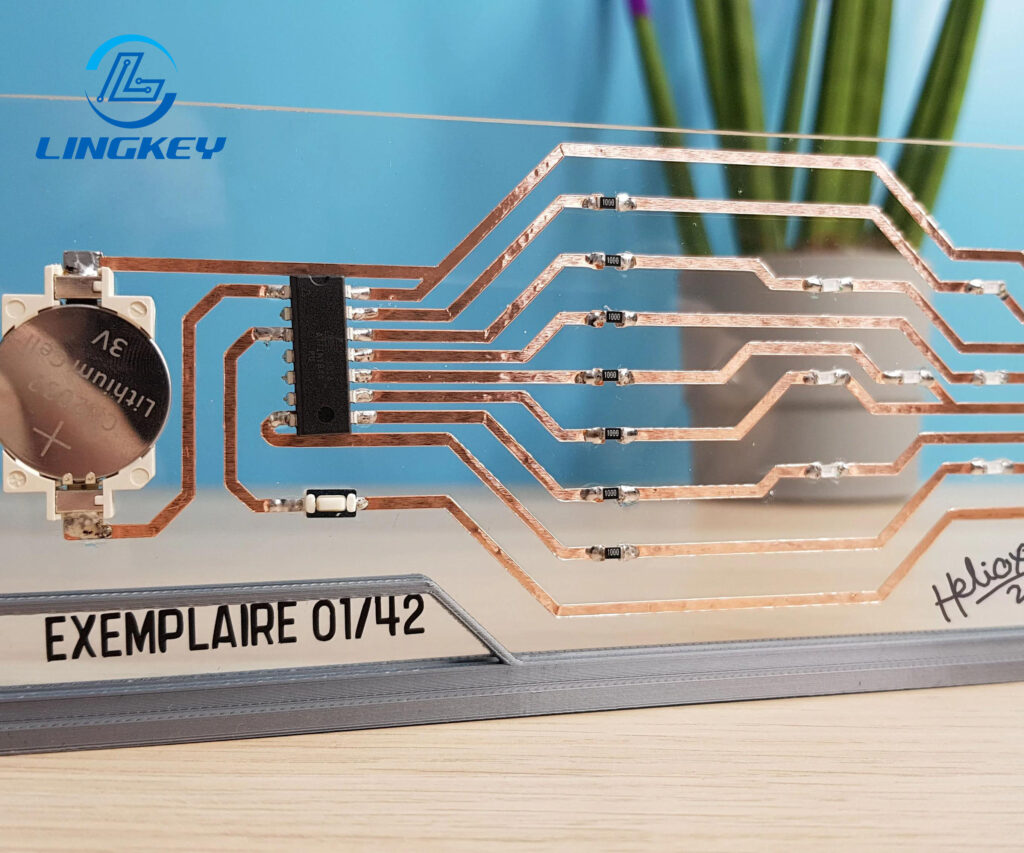
Transparent PCB is a circuit board, manufactured using transparent or semi-transparent material that let the visible or other wavelength of light through. Instead of traditional opaque substrates such as FR4, transparent PCBs are made using glass, polyimide, PET, polycarbonate, PMMA, or even sapphire glass as a base material. The result is an all transparent or semi-transparent printed circuit board which optically and electrically integrates both sides.
Why Use Transparent PCBs?
Transparent PCBs are made for high density layout, high performance, high reliability and visibly appeal. These enable designers to design transparent electronics that allow users to view the circuitry through the body of the device. Transparent PCBs can be used for transparent displays, illuminated touch control, wearable smart devices and futuristic LED solutions.
Materials Used in Transparent PCBs
Selection of the right base material is crucial in making transparent PCBs. Here’s a breakdown of the most commonly used materials:
Material Type | Properties | Typical Applications |
Glass Substrates (tempered, sapphire, regular glass) | Highest optical clarity, rigid, stable | Transparent displays, display covers, lighting, glass PCB |
Transparent Polyimide | Flexible, lighter than glass, moderate clarity | Wearable electronics, flex PCB applications |
PET/Polycarbonate (PC)/PMMA | Flexible, cost-effective, visually transparent | Backlit nameplates, transparent FPC, LEDs |
Ceramic (certain transparent types) | Thermal management, partially transparent, rigid | Power LED, high-frequency, harsh environments |
Glass Fiber (clear variants) | Durable, semi-transparent | Specialty PCBs, advanced electronic design |
Liquid Crystal Polymer (LCP) | Stable for high-frequency signals, transparent or semi-transparent, flexible | RF circuits, transparent PCBs in sensors |
Transparent conductive materials are also essential. Transparent PCBs often use:
- ITO (Indium Tin Oxide)
- Silver nanowires
- Graphene
- Transparent copper meshes
These serve as a substitute for standard copper in conductive traces and do not block light. With transparent conductors such as ITO or silver nanowires, one can form the desired circuit pattern that is still almost invisible.
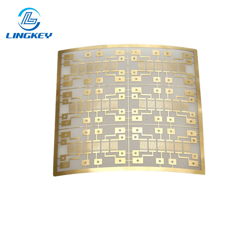
Types of Transparent PCBs
Transparent PCBs come in different forms, depending on their base material and flexibility level:
Glass PCB / Transparent Glass PCBs: They are made of transparent material (usually tempered glass or sapphire glass for higher strength) and are employed in situations that require the highest level of optical clarity and stability.
Ceramic Transparent PCBs: Certain transparent ceramics (such as sapphire or advanced crystal ceramics) offer better thermal dissipation for high frequency signals and rugged conditions, but they might not be totally transparent.
Transparent Flexible PCB (Transparent FPC): Consisting of PET, polyimide, or PMMA, these boards are significantly lighter than glass and enable flex PCB applications in wearables, flexible displays, and space constrained electronics.
Hybrid Designs: Certain designs employ combinations, such as using a glass PCB core with flexible transparent layers to have compact and robust transparent electronics.
Table: Comparison of Materials Used in Transparent PCBs
Feature | Glass | Polyimide | PET/PC/PMMA | Ceramic | LCP |
Clarity | Excellent | Good | High | Moderate | Good |
Flexibility | None | High | Medium-High | None | High |
Weight | Heavy | Light | Light | Moderate | Light |
Thermal Conduct. | Good | Average | Average | Excellent | Good |
Unique Use | Display | Wearables | LEDs/Labels | Power/LED | Sensors/RF |
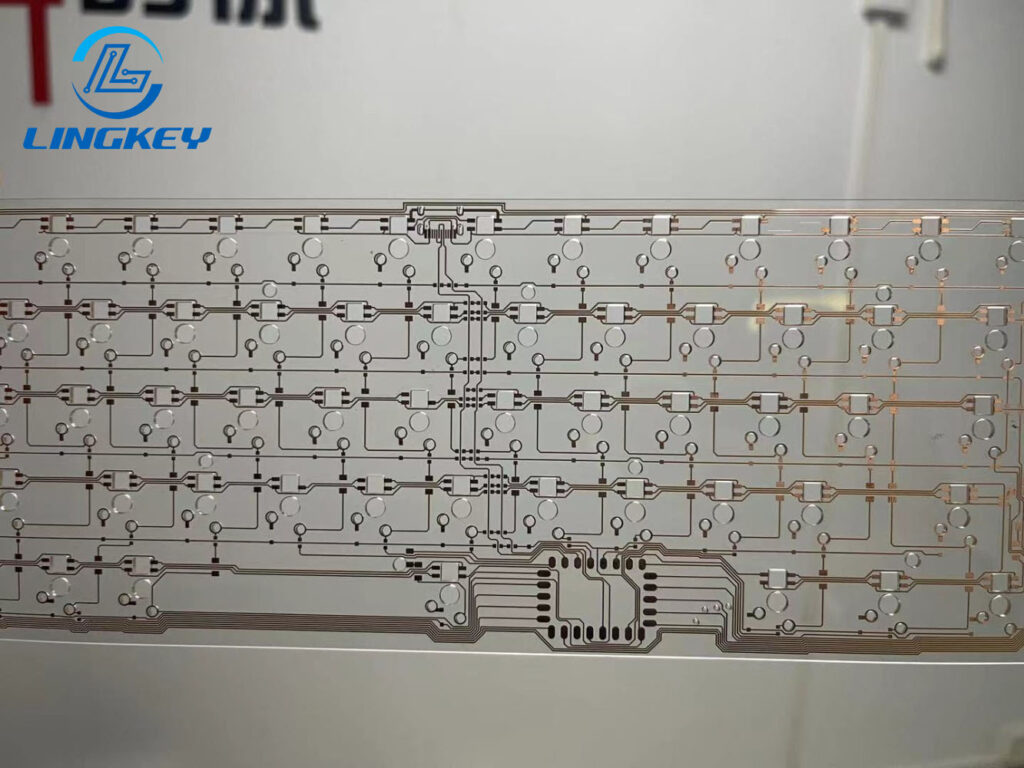
Transparent PCB Fabrication: Manufacturing Process
Production of transparent PCBs The standard PCB manufacturing process is modified for maintaining optical clarity:
Base Substrate Selection: Transparent PCBs are made up of materials such as tempered glass, sapphire, polyimide, or PET depending on the required board thickness, flexibility, and optical requirements.
Transparent Conductive Traces Application: Techniques including sputtering, printing or laser etching, transparent conductive materials such as ITO, silver nanowires or graphene are deposited in the required design circuit pattern.
Photolithography for Pattern Creation: Compliant with meticulous design requirements to form traces without smearing or spreading of light.
Etching and Finishing: Removes undesired conductive material without leaving residue that interferes with clarity.
Board Assembly: In certain constructions, the solder masks are transparent or semi-transparent and special adhesives are used.
Inspection and Quality Control: Ensures both electrical performance and maintenance of optical clarity.
Transparent PCB manufacturing requires higher accuracy as any minor production defects become visible. The PCBs are carefully designed so that they don’t scatter or absorb light – meaning that transparent PCBs can be used with transparent displays and the most advanced lighting solutions.
Design Rules and Considerations for Transparent Boards
Transparent or semi-transparent circuit boards have unique design rules due to their materials and function:
Trace Width & Spacing: Employ the minimum linewidth consistent with the chosen TCM—wider for ITO, narrower for silver nanowires or graphene.
Board Thickness: Glass PCB needs minimum thickness of board for strength as whereas flexible PCB with ultra thin PET or polyimide as substrate, which makes lighter board.
Bend Radius (for flexible PCBs): Make sure the design meets the minimum bend radius to avoid stress fractures in the traces.
Circuit Design: Work for maximum optical transmission by placing traces where they won’t be blocking active areas of light.
Mechanical Support: Some transparent PCBs are stiffened or laminated with conventional glass or glass fiber layers to strengthen them.
Thermal Management: Ceramics or glass are used for high-power applications, plastics for flexible, lower-temperature applications.
Unique Design Benefits: Boards enable designers to add custom shapes, holes, or cutouts for both form and function.
Advantages and Benefits of Transparent PCBs
Transparent PCBs offer design benefits that drive their adoption in electronic design:
- Boards are transparent so they can be used for displays, lit touch buttons, and embedded sensors.
- Compact designleads to thinner devices without additional light pipes or elements.
- Transparent PCBs are lighter than glass when employing polymeric substrates—making them suitable for portable electronic and wearable applications.
- Transparent PCBs reducethe need for connectors or wiring in visible areas.
- With transparent conductive materials such as ITO, both circuits and displays can be formed on a single substrate.
- Visually transparent board designsprovide branding and aesthetic opportunities (e.g., clear smartphone backs).
- High-frequency and RF circuits benefit from ceramic and glass substrates’ electrical performance.
- Transparent PCBs in wearableand flexible electronics enable new applications not possible with opaque boards.
Disadvantages and Challenges of Transparent PCBs
Despite their advantages, transparent PCBs often face several challenges:
- The production of clear PCBs may be more costly due to high cost of materials used in clear PCBs, and tighter process controls.
- Transparent conductive materials such as ITO are not as conductive as copper and may necessitate larger traces.
- The transparent homeland may be more fragile (glass, ceramic) or more susceptible to aging (plastics), depending on the environment.
- Transparent PCBs require advanced processes and must be handled meticulously to avoid visible defects and the entry of foreign matter, so the transparent PCBs can be used only for products in which appearance or special function can be applied.
- Some transparent PCBs come with limitations in power handling and flexibility, especially when compared to specialized traditional flex PCBs using copper.
- The selection of base material—glass, polyimide, PET, or sapphire glass—could influence the compatibility with the current electronics manufacturing lines and may need customized solutions and process modifications.
Applications: Using Transparent PCBs in Modern Electronics
Transparent PCBs are tailored to address the requirements of high end electronic design and they are applied in areas in the application field of optical solutions, where the optical path and a small-size package are of significant importance. Key areas include:
- Transparent Displays:Application in futuristic billboards, dashboard heads-up display (HUD) in vehicles, and consumer electronics of the new era.
- Wearable Devices:Transparent or semi-transparent boards enable lightweight, comfortable, and visually distinctive smart wearables.
- LED Lighting:Boards are translucent, which light can pass directly through the substrate, allowing for uniform, edge-lit effects in architectural and automotive
- Medical Devices:Transparent PCBs in wearable or implantable sensors seamlessly integrate with the skin, increasing patient comfort and assist in optical-based diagnostics.
- Flexible Electronics:Flexible PCB are available in rollable, foldable or curved products which are not possible with rigid, solid boards.
- Backlit Touch Controls:Device with touch sensors, lighting, and display on one transparent substrate for visual appearance and functional integration.
- Transparent Electronics:Emerging fields like smart windows or see-through consumer appliances often use transparent PCBs as core components.
Transparent PCBs are usually made with high performance materials such as glass, sapphire glass, and clear polyimide to accommodate these high level demands, which allows for products that were unthinkable 10 years ago.
Transparent PCB vs. Traditional PCB
Here’s a detailed comparison to highlight where each technology excels and where transparent circuit boards give your design an edge:
Feature | Transparent PCB | Traditional PCB |
Substrate / Base Material | Glass, sapphire, polyimide, PET | FR4 (glass fiber + epoxy) |
Optical Clarity | Transparent or semi-transparent | Opaque |
Conductive Traces | ITO, silver nanowires, graphene | Copper |
Flexibility | High (plastics); None (glass) | High (flex); None (rigid) |
Suitability for Light/Display Uses | Excellent | Poor |
Weight | Lighter than glass (plastics) | Standard |
Cost | Higher (materials/process) | Lower (mass production) |
Manufacturing Process | Custom, precision-critical | Standardized |
Design Benefits | Compact, visually transparent, advanced features | Mature, robust |
Durability | Careful design required | Rugged (especially FR4/Cu) |
Environmental Impact and Future Trends
Environmental Considerations
The manufacture of transparent PCBs is usually with special materials and chemicals, thus causing difficulties for recycling or molten processing. However, novel investigations are being carried out to produce transparent PCBs using green, recyclable polymers and alternative conductive inks that minimize environmental detriment.
The Future of Transparent PCBs
- Transparent PCBs will playa central role in transparent electronics, AR/VR, smart windows, and display technologies.
- Developments in transparent conductive materials (e.g. graphene, carbon nanotubes) and fabrication of transparent PCBs are enhancing conductivity as well as sustainability.
- With improved reliability and cost reductions, using transparent PCBswill expand to even more compact design electronics and wearable devices.
- New hybrid technology, like boards with flexible and rigid transparent sections, will bring even greater unique design advantages to innovative products.
FAQs about Transparent PCBs
What is the key advantage of using transparent PCBs in consumer electronics?
Are transparent PCBs always made from glass?
Can transparent PCBs replace all traditional PCBs?
Can you make multi-layer transparent PCBs?
What applications benefit most from transparent PCBs?
Conclusion
Transparent PCBs integrate form and function and allow for a new era of smaller, eye-catching, and very functional electronic devices. Based on clear glass, high performance transparent polymers, and novel transparent conductive materials, these substrates provide light transmission while enabling the reduction of feature sizes and introducing new ways of thinking in industrial design for applications from flexible electronics to IoT devices.
With the development of transparent and translucent electronics, effective realization is getting more reliant on materials selection, optics-aware design of circuits, and process control in optics during fabrication. Herein, mature PCB fabrication companies like LingKey help to support this by converting transparent PCB ideas into real-world hardware that is manufacturable and dependable – balancing optical clarity, electrical function and production feasibility.
As the interest for transparent displays, wearable electronics, and next-generation human–machine interfaces grows, the transparent PCB materials and processes will continue evolving, enabling wider commercial applications and more complex product designs.
")
")


")
")
")


