What Is DIP Soldering? The Complete Guide to DIP Solder
Table of Contents
ToggleIntroduction
Solder is a fundamental requirement of modern electronics manufacturing. From large-scale production facilities to garage workspaces, the need to establish reliable electrically connected joints between components and PCBs (Printed Circuit Boards) remains essential. Although SMT (Surface Mount Technology) and SMD (Surface Mount Devices) have revolutionized miniaturization and automation, the DIP soldering technique continues to be important, in particular for rugged, high-current apparatus, prototype assembly, and industries that demand a robust and dependable design.
This detailed guide contains an detailed report how dip soldering is strong and flexible, why you are still using dip soldering in new build, and how this technology enables dependable solder joints even in harsh environments.
What Is DIP Soldering?
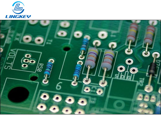
DIP soldering is one of a variety of PCB assembly processes and is used to solder through-hole components like dual in-line package (DIP) integrated circuits onto a PCB. The technique consists of placing the leads of components into through-holes and then establishing a solid mechanical and electrical connection by means of molten tin-based solder.
Unlike SMT, where the SMDs are directly placed on the surface, the holes serve as dedicated columns anchoring each component in DIP soldering, which delivers excellent mechanical stability—a requirement for power devices, electrolytic capacitors and the like where reliability is critical. It is the heart of PCBA (printed circuit board assembly), particularly for units designed to resist vibration, high current, or recurring service.
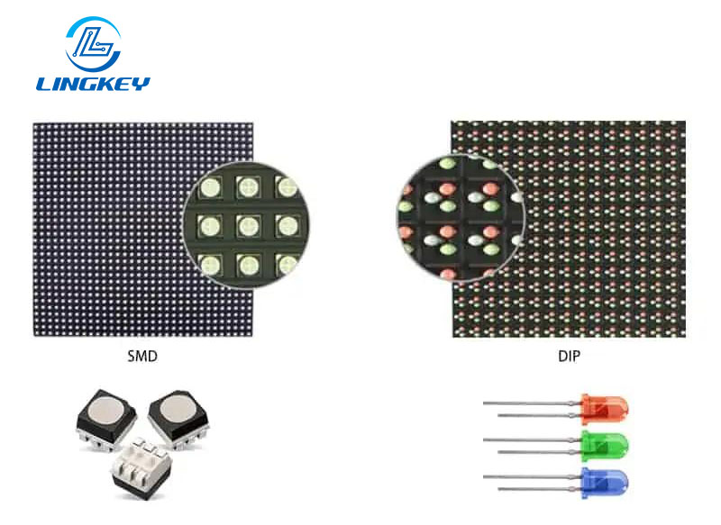
Overview of DIP Components

Types of DIP Components
The DIP (Dual In-line Package) components are still used in electronic manufacturing both old and new. Some common examples are:
- Integrated Circuits (ICs):Microcontrollers, logic gates, and memory chips.
- Passive Component Networks:Arrays of resistors/capacitors in standard DIP formats.
- Electrolytic Capacitors:Used for filtering and power stabilization, especially in DIP-based power devices.
- Electromechanical & Electro-Optical Components:DIP switches, relays, and opto-isolators.
- Interface & Configuration Components:DIP switches and jumpers for device customization.
By lead form, you’ll encounter:
- Standard DIPs:Parallel rows of straight leads.
- SIP (Single In-line Package):A single row for denser layouts.
- ZIP (Zig-zag In-line Package):High pin density for complex circuits.
- J-Leads:Underneath-bent leads, allowing a lower profile and better alignment.
DIP Package Characteristics
DIP packages are standard so the pin spacing and numbering is predictable. Most of them have 0.1-inch spacing (2.54 mm) and very rugged thermally stable body which act as heat sink. Through-hole DIP components are therefore particularly useful when dealing with high current, voltage, and mechanical abuse.
Markings and Orientation
Reading and installing DIPs correctly is vital. Component bodies include:
- A notch or marker indicating Pin 1.
- Manufacturer and part numbers (important for sourcing and repairs).
- Date or lot codes for quality assurance.
Proper orientation ensures electrical and mechanical integrity, and avoids disastrous failures at power on, as well as allows you to take out and put in bad parts with confidence.
The DIP Soldering Process: Step-By-Step
Creating reliable solder joints with DIP soldering involves these critical phases:
Preparation Work
All the through hole parts and pvc are wiped with a run of isopropyl or de-ionized water to clean away dust, oil, and oxides. An ESD safe environment is created to eliminate the potential for latent defects. Collect your materials: solder paste (if doing hybrid assembly or prepping for wave soldering), tin/lead or lead-free solder wire, flux, and clipping tools.
Component Insertion
Plug each DIP element into its corresponding hole on the PCB. Keep pins aligned and verify labels and positioning. A good fit reduces defects such as bridging and also allows for removal at a later time.
Soldering
With components seeded:
- For hand soldering, heat the pad and lead then apply the wire of solder. Liquid solder flows out through the hole, filling the space and making a strong and dependable connection.
- For mass production, run the loaded board through a wave soldering machine. In this wave soldering process, a conveyor transports the PCBA over a solder pot where a “wave” of molten tin comes in contact with all exposed, plated through-holes, resulting in effective and dependable multipoint connections in a single step.
- Selective solderingmay be used for high-density mixed-technology boards to solder only certain areas or specific through-hole components.
Lead Trimming and Cleaning
Cut away the protruding leads under the board to prevent shorts and for a better finishing. Clean up the flux residue with isopropyl or deionized water by rinsing and drying for long-term electrical reliability.
Inspection and Quality Control
Examine each joint carefully for cold solder joints, cracks, excessive amounts of solder, or other imperfections such as bridging. Solder fillets should be smooth and shiny; a good joint flows around the lead and the pad. AOI, X-ray and functional test for complex or high reliability PCBA.
At LingKey, DIP solder joint inspection is performed per IPC-A-610 standards, with the aid of AOI, X-ray inspection, and functional testing to maintain uniform quality in both prototype and volume production.
DIP Soldering Methods
Manual (Hand) Soldering
Employed for prototyping and small-scale production runs, this technique enables technicians to directly bond to form robust and dependable connections and to rapidly modify or mend circuits. It’s just slower and you need skilled people.
Automated (Wave Soldering)
Wave soldering is fast and consistent. A wave soldering machine can solder thousands of through hole leads in seconds guaranteeing a perfect double wave soldering every lead is surrounded with molten solder on both underside and upperside from the solder reservoir. The process is very repeatable and can be tailored for both leaded and lead-free solder alloys.
Selective Soldering
For mixed-technology (SMD + DIP) boards, selective soldering restricts the soldered area to through-hole components only. This process of dip soldering includes programmable solder nozzles, minimizing risk to adjacent SMT assemblies.
DIP Soldering vs. Surface Mount Technology (SMT/SMDs)
Feature | DIP/Through-Hole | SMD/SMT |
Mounting Style | Pins through PCB holes | Pads on surface |
Soldering Technology | Wave, manual, selective | Solder paste, reflow ovens |
Board Space Usage | Larger footprints | Miniaturized circuits |
Mechanical/Power Handling | Very robust, high-current | Less robust, low-current |
Repairability | Easy to remove and replace | Difficult, needs hot air |
Cost (High Volume) | Higher | Lower |
While SMDs allow for complicated circuitry and extremely small products, utilize dip soldering in high-current devices or critical control modules in which the electrical connections must be reliable.
Advantages of DIP Soldering
A few reasons to still use DIP soldering in PCBA:
- Electrical and Mechanical Strength: Through-holes and large solder pads make joints withstand stress, which is essential for power supplies, relay boards, high-current devices or critical control.
- Easy to Remove and Replace:Faulty or outdated parts are straightforward to desolder and swap, reducing downtime and scrap.
- Efficient and Reliable for Specific Applications:Especially in industries like automotive and aerospace, where reliable electrical and physical connections are non-negotiable.
- Solder Multiple Components Quickly:Wave soldering equipment allows to solder large quantities of through hole parts at the same time resulting on even processing in production and the efficiency of production planning for these assemblies such as relay boards and filter banks.
- Versatile for Prototyping and Design Changes:Through-hole parts, particularly DIP, can be swapped easily while debugging and prototyping, which speeds up the development of robust and reliable electronic circuits.
Limitations of DIP Soldering
While DIP soldering provides many strengths, it is not a universal solution in modern electronic manufacturing:
- Lower Integration and Miniaturization:DIP and through-hole parts take up more space on a PCB, constraining how small/complex a board can be.
- Increased Production Cost and Time:The process requires manual placement or additional tooling and is less amenable to full automation than SMT.
- Unsuitable for Complex, High-Density Boards:SMT/SMD and solder paste application allow for even higher levels of integration and are thus the choice for high density, multi-layer PCBs in mobile and consumer electronics.
- Thermal Stress and Soldering Challenges:DIP soldering problems can be caused by thermal expansion and contraction, leading to cracks or mechanical damage if hurried or otherwise badly controlled.
- Potential Defects:Problems such as cold joints, too much or too little solder, and defects like bridging may arise if process controls—solder reservoir temperature, preheating, and fluxing—are lax.
Applications of DIP Soldering in Electronics
Despite its limitations, DIP soldering remains indispensable in:
- Automotive Electronics and Power Devices:Modules of high reliability, relay matrices and power regulation circuits are benefited by robust through-hole connections.
- Industrial Automation:DIP packages are selected for PLCs, IO modules and control systems where field repairability and ruggedness are important considerations. Aerospace, Military, and Harsh Environments: DIP soldering results in a strong and dependable electrical and mechanical bond on application specific control boards.
- Educational Kits and Prototyping:DIP components are easy to solder, remove and replace, so they are ideal for learning environments and quick development.
- Electrolytic Capacitors and Large Inductors:Through-hole mounting allows heavier, more expensive components to be used that would be unable to be securely attached to a circuit board just using the SMD pads.
These are the application areas very similar to the PCB assembly experience of LingKey, in which DIP soldering is common in power electronics, industrial control boards, and assemblies for the mission-critical are designed for higher durability.
Quality Assurance in DIP Soldering
Effective DIP soldering is defined by:
- Visual Inspection:Magnifiers or AOI are employed to verify a good soldering joint—shiny, full fillets, with no visible voids or bridging.
- X-Ray and Functional Testing:PCBA needs to be tested with concealed connections or layers of stacked PCBA to reveal the hidden cold joints or shorts.
- IPC-A-610 Standard Adherence:This industry specification describes the requirements for quality of the PCBA, including definitions for tin coverage, lead protrusion and defect classification.
- Reliability Testing:Boards can be exposed to thermal cycling, vibration, and moisture to guarantee stability under service.
- Cleaning:Using deionized water, flux and contaminants are removed, which minimizes the potential for corrosion and allows for a high level of processing and product reliability during the life of the product.
Best Practices & Common Mistakes in DIP Soldering
Best Practices:
- Use high-quality solder wire or paste, with adequate flux to aid wetting.
- Control temperatures rigorously during wave soldering—overheated boards risk delamination, while insufficient heat produces unreliable joints.
- Maintain ESD-safe environments, especially for sensitive ICs.
- Always verify the orientation and seating of DIP components before soldering.
Common Mistakes:
- Inadequate Soldering:Cold, dull joints signal weak or incomplete soldering.
- Excessive Solder:Can cause bridging between pins—use a solder wick to remove excess.
- Inconsistent Lead Trimming:Leads cut too long risk shorts, too short risk mechanical weakness.
- Skipping Cleaning:Leftover flux leads to circuit failures, especially in humid conditions.
DIP Soldering Rework, Repair, and Desoldering
One of the best aspects of DIP soldering is that you can easily desolder and replace problematic through-hole parts.The procedure usually consists of:
- Solder Sucker/Solder Wick:Used to extract molten tin from through-holes, freeing the leads for removal.
- Hot Air or Desoldering Stations:For large components or those sensitive to heat, a controlled flow of hot air is used to gently melt the solder without harming the pad or the component.
- Component Replacement:After removal, clean the site, replace with a new part and reflow, making certain that the new joint meets all the requirements for reliability.
The robust and predictable nature of this repair and refurbishment process prolongs the life of power devices and critical assemblies.
Frequently Asked Questions About DIP Soldering
What’s the main reason to use dip soldering in modern electronic manufacturing?
How does a wave soldering machine ensure quality?
Are there best practices for cleaning after the DIP soldering process?
How are DIP soldering challenges addressed in manufacturing?
Summary & Final Thoughts
Despite SMD and surface mount assembly now dominating high volume consumer electronics, DIP soldering retains its essential role in modern electronic fabrication, in particular where dependable electrical connections and strong, robust and reliable joints are a must. Knowing dip soldering process, equipment, advantages, challenges and best practices will help you to produce a PCBA, no matter it is for prototypes or high-power industrial devices, which can meet the highest expectation on perfomance and durability.
DIP soldering maintains dependable performance under harsh conditions when process control is disciplined and the right equipment is used. With the best of traditional through-hole soldering methods and modern quality systems, LingKey enables customers to deliver robust, serviceable, and high-reliability PCB assemblies for industrial and power applications.
")
")


")
")
")


