What Is Silkscreen in PCBs?
Table of Contents
ToggleIntroduction
In PCB design and production, the silkscreen on a PCB is an essential but underrated aspect. This silkscreen layer (a thin layer of ink printed on the PCB itself) delivers important information that helps you during assembly and troubleshooting. It prints text and graphics on the substrate of the PCB, helping you more easily identify, assemble and repair your electronics. This comprehensive tutorial covers not only what the silkscreen is and how it is applied but also its importance in the entire process of PCB manufacturing.
What Is Silkscreen on a PCB?
Definition and Role of the Silkscreen Layer
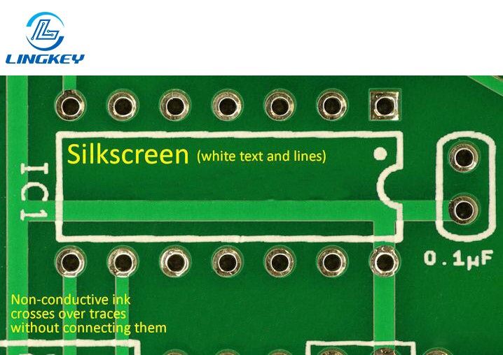
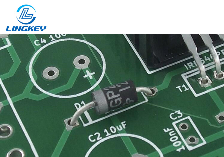
The silkscreen on PCBs, also known as the legend or component print, is a layer of ink that is applied as part of the PCB fabrication process. This is usually printed on the PCB surface and includes human readable text and symbols such as component reference designators (R1, C2) polarity, manufacturer logos, warnings and assembly instructions. The silkscreen layer is non-electrical in nature, its only function is to provide faster identification, less chance of errors and better aesthetics and usability to the board.
Silkscreen is more than just a decorative layer, it is also a communication layer in the pcb assembly process: giving instructions to assembly, both for automated and manual. Whether you are designing a conventional PCB or one of the high-tech kinds, having the right silkscreen for your PCB is essential if you are a pro who needs to know what is going on.
Silkscreen vs Solder Mask
There is a difference when it comes to the silkscreen layer and the solder mask. They are both pcb layers, but for different purposes and applied in different ways.
Feature | Silkscreen Layer | Solder Mask Layer |
Purpose | Visual & assembly info (text/symbols) | Protect copper, prevent solder bridging |
Layer of Ink or Polymer | Layer of non-conductive epoxy ink | Polymer layer (often green) |
Where Applied | Top/bottom surface, over solder mask | Directly over copper traces, except for pads |
Colors | White, black, yellow—high contrast on PCB substrate | Mostly green, some red, blue, black, white, etc. |
How Applied | Exposed via various printing process (see below) | Usually via LPI or spray/squeegee |
Impact on Assembly | Ensures correct placement & easy identification | Ensures proper soldering |
If the solder mask is the protecting layer of the traces and pads, the silkscreen is an additional layer of text on the PCB that helps with the assembly, servicing and compliance.
The Importance of Silkscreen on PCB
The silkscreen layer on a PCB serves more than just as a map for the assembly process—it’s critical for safety, cost effectiveness, and product quality.Talk about silkscreen throughout the life of any electronic product:
- Component Identification The silkscreen on the PCB helps to the component placement accuracy and efficiency for the PCB assembly, that can use for easily both automated machine and technician to reduce error.
- Assembly & Orientation Tips The silkscreen indication for polarized parts such as electrolytic capacitors and diodes provides their orientation on the board preventing reverse placement.
- Diagnostics and Troubleshooting Marked test points and jumpers allow for fast diagnostics so the design can be easily read and debugged.
- Traceability & Documentation Batch codes, revision numbers, and manufacturer logos printed as part of the silkscreen enhance regulatory compliance and process control.
- The Aesthetic & Brand Logos, batch information and certifications printed on the silkscreen help elevate the professionalism and serve as crucial legal information.
- Safety Indicators Warnings and polarity markers silkscreened to comply with safety regulations and protect the user and the operator.
Silkscreen offers the PCB orderly information that Bolsters from processing and test to each assembling and troubleshooting in the life of the device.
Information Printed on the PCB Silkscreen
The silkscreen is a layer that can contain many types of markings, which are usually customized in the process of PCB designing and manufacturing:
Common Silkscreen Markings:
- Reference designators for components on the PCB (R, C, U numbers)
- Orientation (pin 1/polarity for ICs, LEDs, capacitors)
- Test point identifiers for pcb testing
- Manufacturer’s logo, batch numbers, or production codes for traceability
- Certification and compliance marks (e.g., CE, RoHS)
- Text and symbols for connectors, switches, mounting holes
- Safety warnings on PCBs(e.g., high voltage, static sensitive areas)
Properly designed silkscreen layers can significantly ease the assembly and testing phases of electronics lifecycle management.
Materials and Properties: What Is Used for Silkscreen PCB?
Non-Conductive Epoxy Ink & Color Options
Silkscreened inks for PCBs need to be non-conductive so that they don’t create interference or shorts. The most used is the non conductive epoxy ink that have good adhesion on the surface of pcb and the resistance to heat and chemicals in the process of pcb making. Other alternatives are UV-cured inks which have great definition and fast curing times.
Popular colors for silkscreen include:
- White:For high contrast on traditional green solder mask.
- Black:For white or lighter boards.
- Yellow:For special visibility demands The color selection is made by contrasting with the background pcb substrate so that the data can be read easily.
Silkscreen Thickness and Durability
A good silkscreen is only as good as its use: the ink layer must be thin enough (around 0.1 mm) to not interfere with the assembly but thick enough to withstand the handling and environmental conditions. The heat and chemical resistance of the ink allows the ink to be durable both in the process and the end of the pcb assembly. Sticking properly to the PCB is vital – a poorly adhering ink may cause smudged markings or contamination.
PCB Silkscreen Printing Techniques
Manual Screen Printing
It is the manual screen printing of PCB solder paste, that directly affects PCB quality during the assembly, because it is apparent that printing is the most important part of the process and can pave the way for the rest of the assembly. While cheap and widely used for mass production of simple boards, manual printing has its limitations when it comes to producing fine or complex patterns.
Liquid Photo Imaging (LPI)
LPI is the photographic process of applying pcb solder mask by straining the pcb with uv light through a film which has been imaged with pattern. The parts that are exposed to the UV become hard and this forms the picture. This technology enables much finer silkscreen and is now available as standard in both standard and high-tech PCB processing.
Direct Legend Printing (DLP)
Direct Legend Printing (DLP) places UV-curable ink directly on the layer of the printed circuit board using an inkjet printer. It is the very process that enabled digital files to be rendered with great fidelity on the PCB, allowing for quick turnarounds, and high-resolution marking during printing.
Advanced Silkscreen Innovations
Modern PCB manufacturing often integrates:
- Dry Film Silkscreen:For ultra-fine features.
- Laser Direct Imaging:For ultra-HD text, minimizing risk of errors in tiny pitch designs.
- Automation in Printing:Robotics and vision systems enable the silkscreen to be applied accurately and uniformly, helping to maintain high manufacturing quality and to minimize human error.
- 3D Printing:Some advanced silkscreen PCB techniques now leverage 3D-printed layers, which can add tactile or enhanced visual cues to a PCB.
- Conductive Inks:Continuous investigations to apply silkscreen utilizing conductive inks will potentially open up new applications in future, but in today’s PCB most silkscreen is non-conductive.
PCB Manufacturing Process: How to Apply the Silkscreen
There are multiple steps in making a silkscreen in your PCB including some that are all important to guarantee that the silkscreen will stick to your PCB and looklike good below is a typically simple outline of how silkscreen onto the PCB is embedded with the rest of the PCB production process:
Designing the Silkscreen: In the initial design stage the silkscreen layer is generated within the PCB design software. Designers also make a careful selection of the text and symbols that can be printed to remain clear and legible within space constraints.
Exporting Gerber Files: The design is exported as a Gerber file, which has all the layers (including the silkscreen) required to produce.
Applying a Solder Mask: A layer of solder mask is applied over the copper traces before silkscreen is printed. This layer of polymer isolates and shields circuits and is the base for subsequent silkscreen deposition.
Applying the Silkscreen: Based on the choice of silkscreen pcb printing method (manual screen printing, LPI, or DLP), the ink is either forced through a stencil, photo-imaged, or printed on the solder-masked surface of the pcb. This method of printing is important to make sure that the silkscreen is a layer that both sticks firmly to the surface of the pcb and is clear enough to be useful when assembling and troubleshooting.
Curing the Ink: After the ink is applied, the PCB undergoes thermal or UV curing, which solidifies the ink layer so that it adheres well to the PCB and can resist the heat and chemicals of subsequent assembly processes.
Inspection and Quality Control: Automated Optical Inspection (AOI) and manual inspections verify that the entire information printed on the pcb is accurate, readable and well-aligned, and silkscreen is not covering soldering pads or important copper stack.
PCB Assembly Process: Once the silkscreen layer is done, the PCB goes to the main assembly, where the components are placed and soldered with the help of the markings on the silkscreen layer that help on preventing mistakes and facilitate the assembly and maintenance of the device.
Designing the Silkscreen for Your PCB
Creating the silkscreen layer your PCB is a technical challenge, and a bit of a creative one too. The goal is to make everything as easy to read and use as possible, without making the board feel crowded.Here are a few best practices:
- Plan Placement Early: Determine what information is most needed for assembly and to diagnose problems during the assembly, e.g. part reference designators, orientation indicators, and safety symbols.
- Choose Fonts and Sizes Wisely: Use sans serif fonts with a minimum font size of 1.0 mm and line width (stroke width) 0.2 mm for the Silkscreen layer to keep the silkscreen readable after it’s printed on the PCB.
- Prioritize Contrast: Choose a contrast color pair (white on green, black on white) so that information on the pcb can be read under any lighting condition.
- Avoid Functional Interference: Should be no silkscreen on exposed copper pads, vias or traces to avoid assembly problems
- Follow Compliance Standards: Comply with IPC-2221 and other standard for the text, size of symbol and space.
- Update During Revisions: If the assembly or parts on the pcb get changed, review and update silkscreen layer to not leave old or misleading markings.
Ensuring Silkscreen Quality in PCB Production
There must be rigorous quality control in the whole process of pcb fabrication to guarantee the silkscreen is correct and enduring.Quality inspections will:
- Verify all legends and symbols are present and legible.
- Confirm silkscreen adheres properly to the pcb and does not flake during handling.
- Ensure that the layer of ink does not compromise solderability or cause rework.
AOI systems and seasoned technicians examine each and every board (except the SMT process for the bottom side) thoroughly, fixing any errors before the mass production assembly.
Innovations & Trends in Silkscreen PCB Printing
Recent developments are changing the way the silkscreen layer is produced on an electronic board:
- Repeatability is assured with Printing Automation, which enables the mass production of uniform and high-quality PCBs.
- UV-cured Inksextend the life of silkscreen under harsh environmental stresses.
- Laser-cut Stencilsprovide intricately detailed patterns for highly advanced silkscreen applications.
- Integration with Design Software enables font size, presence overlap with pads, and white space checks to be performed automatically during the design stage, resulting in enhanced first-pass yield and reduced turnaround time.
These trends make the silkscreen application and silkscreen design flow naturally as part of the overall PCB design and manufacturing process.
FAQs About the Silkscreen PCB Layer
Can a PCB be produced without a silkscreen layer?
What’s the most durable method for applying the silkscreen?
Is it possible to print silkscreen on both board sides?
Conclusion
The silkscreen of a PCB is not only visual aspects—it is essential for whole the PCB manufacturing process and an significant layer to quick, easy, good assembly, diagnosis, maintenance, and compliance. Correctly designed silkscreen for standard PCBs as well as high-speed digital designs ensures assembly without error and long-term reliability. As you continue to get deeper into designing and fabricating pcb’s, make sure the silkscreen on all your projects is crisp, clean and you keep an eye on it!
The silkscreen design, print accuracy and inspection standards are strictly controlled from the beginning which can be guaranteed by cooperating with professional PCB manufacturer like LingKey, so that the end product will be professional, reliable and easy-readable PCB that you could rely on for multiple years.
")
")


")
")
")


