Why are 3 layer pcb designs so rare?
Table of Contents
ToggleIntroduction to 3 Layer PCBs
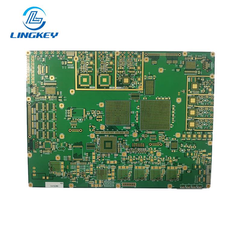
The construction of PCBs can vary from a single board with only one layer of copper to multilayer PCBs with intricate armature structures. Standard designs are 2-layer and 4-layer multilayer pcbs, however the 3 layer pcb (or 3-layer board) is an uncommon exception. This is a bit strange since three layers of conductive copper foil may seem, on paper, to provide more functionality at a lower cost of materials. But since 3-layer PCBs are nonexistent, the truth is 3-layer PCBs is anything but straightforward.
Although 3-layer PCBs seem appealing in theory, they need to be appropriately engineered in practice. At LingKey, PCB engineers often review odd-layer designs for early DFM discussions, but in the vast majority of cases they suggest different layer stackups that offer improved mechanical stability and signal integrity without raising cost or risk.
Why Focus on the 3 Layer PCB?
Most multilayer board designs use an even number of layers for electrical and mechanical reasons. But with increasing demand for miniaturization in products such as smartphones and high-density electronics, design engineers occasionally look into odd-numbered solutions. This paper investigates the reason why 3 layer PCB is rarely used, what the problems faced in lamination and mechanical performance, and when the 3-layer board offers the best value.
How a 3 Layer PCB Is Built: Stackup, Structure, and Components
Designing a 3-layer PCB is a balancing act of meeting electrical requirements and structural requirements. Let’s look at the structure of such a design for these special PCB boards.
Typical 3 Layer PCB Stackups
A PCB stack-up is the relative arrangement of a number of copper layers and insulating layers in a PCB. In a 3-layer PCB, these are some most popular layouts:
Stackup Type | Top Layer | Inner Layer (Middle) | Bottom Layer | Description |
Signal / Ground / Signal | Signal | Ground Plane | Signal | One ground plane sandwiched by signal layers |
Signal / Power / Signal | Signal | Power Plane | Signal | Middle power layer improves distribution |
Signal / Signal / Signal | Signal | Signal | Signal | Maximum routing, poor reference paths |
Each build begins with copper foil laminated to various substrates—most commonly FR4 or polyimide— which are then bonded and pressed under heat and pressure in the lamination process.
Materials Used in a 3 Layer PCB
Different materials provide different benefits to PCB layers.
- FR4: The most common, providing good thermal and electrical performance for most applications.
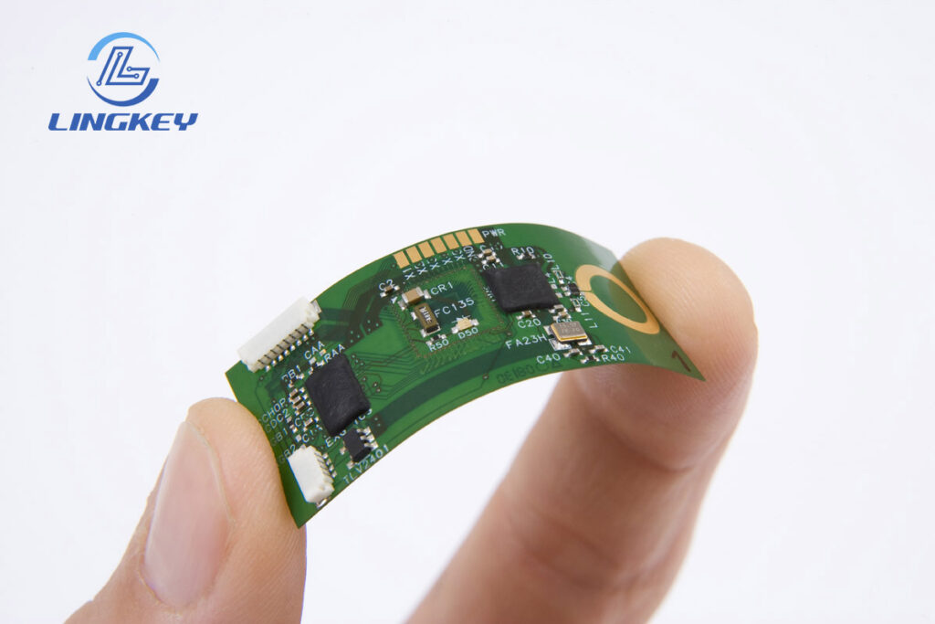
- Polyimide: Ideal for flex circuitsdue to its flexibility and heat resistance.
- PTFE: Used for high-speed or RF boards.
The layers of copper foil in each conductive layer need to be accompanied by layers of insulation for electrical isolation and for the multilayer PCB design to work.
Components on 3 Layer PCBs
Although the routing is limited by the layer arrangement, all the standard PCB parts can be used:
- Surface mount and through-hole devices
- Sensors, resistors, capacitors, diodes, transformers
The component placement on the top and bottom layers needs to be balanced for heat and mechanical stress.
Thickness and Layer Structure
The final size of the three-layer board is controlled by:
- Core (between layers)
- Prepreg thickness(bonding insulation)
- Thickness of copper foil
Typical thickness is usually around 0.7 mm for compact, lightweight 3-layer PCBs, but there are options for custom thicknesses. This thinness can lead to warpage if the symmetrical balance is not meticulously adhered to between each outer layer and the single inner layer.
Why 3 Layer PCBs Are Rarely Used
The reason which leads to the rarity of 3-layer PCB in the industry might be the combination of mechanical, electrical and economical considerations.
Asymmetric Structure & Warp
Odd-layer count boards (e.g. 3-layer PCBs) are inherently asymmetrical. The even-numbered designs create mirror images about the center, while a 3 layer PCB has two outer layers and one inner layer.In the lamination process these packed materials contract at differing rates when cooling:
- Copper and FR4shrink differently, creating stress that causes permanent bending, or warpage.
- The board provides insufficient resistance to these stresses without an internal mirror layer, so 3-layer PCBswarp more than their even-layered counterparts.
Manufacturing Complexity & Quality Control
Making a 3-layer board is not easier than making a 4-layer board. QC is more difficult, tooling is specialized and volume is low.
- Some manufacturers add “dummy” layers to balance the board structure.
- The additional care required during the lamination process increases both cost and lead time with no direct economic benefit compared to standard even-numbered layer PCBs.
Electrical Performance Issues
- In a three layer board, only one genuine ground plane or power plane is achievable which detracts from signal integrity, impedance control and EMI performance.
- High-speed traces do not have solid reference paths, and thus those PCBs are not suitable for critical analog or digital circuit.
3 Layer PCB vs. 2-Layer, 4-Layer, and Multi-Layer Boards
PCBs are functional, performance, and cost-driven design decisions. Here is how 3-layer PCBs compare:
Feature | 2-Layer Board | 3-Layer PCB | 4-Layer Multilayer PCB | Multi-Layer PCBs (6+) |
Routing Flexibility | Low | Medium | High | Exceptional |
Warpage Resistance | High | Low (prone to warp) | High | High |
EMI/Signal Integrity | Fair | Risky | Good | Very Good–Excellent |
Ground/Power Planes | None/1 | 1 | 2 | Multiple |
Production Cost | Low | Medium–High | Nearly same as 3-layer | Higher |
Application Fit | Simple circuits | Rare/prototyping | Phones, IoT, automotive | Servers, High-speed, RF |
As above, the “3-layer PCB” is outperformed by its 4-layer counterpart in all aspects, though it does bring some advantages over 2 layers—especially for routing or when space is at a premium.
When Does a 3 Layer PCB Make Sense?
Three layers may sometimes be justified for:
- Prototyping & Custom Flex Circuits:When a designer has to route additional signals in a cramped, dimension-limited area (e.g., wearable medical monitors, modules in devices phones, etc.)
- Rigid-Flex Transitions:with one part of the board being rigid and other part flexible, and a fourth layer would prevent foldability.
- Strict Board Thickness Requirements:When the overall height of the stack must be kept as low as possible (e.g. 7mm), and 4 layers can not be fit.
However, these are exceptions—multilayer boards with an even number of layers are still standard for most advanced applications. In general, 3-layer PCBs are only warranted by special mechanical or layout requirements that cannot be satisfied by a conventional 2-layer board or a thin 4-layer stack.
Advantages and Limitations of 3 Layer PCBs
Advantages
- Extra Routing Density:Compared with a 2-layer board, 3 layers provide more room for routing, which can be very essential in cell layouts.
- Selective Layer Functionality:A ground or power plane may be devoted to the inner layer, enhancing the performance of some signals.
- Space-Saving:When the thickness of a three-layer PCB is critical (for example, in devices such as smartphones), the design can sometimes shave component stacking heights or enable thinner batteries.
Limitations
- Structural Symmetry Issues:The absence of a reflective, uniform organizationismic stress is generated, which in turn leads to mechanical distortions causing the board to bow, primarily when differences in copper density are present between layers.
- Manufacturing Complexity:Extra process steps in the lamination and additional quality control demands contribute to higher cost and production time, which also offset material savings among less layers of copper foil.
- Signal Integrity Concerns:Signal integrity and EMI [electromagnetic interference] are degraded with only one solid reference plane, particularly at higher frequencies.
- Limited Industry Support:There are a few manufacturers that regularly make 3-layer PCBs, particularly with advanced features such as HDI, microvia or special finishes.
Key Design and Manufacturing Considerations
Designers going with a 3-layer PCB need to be disciplined in both layout and material selections.Here’s what to focus on:
- Copper Balance: Make the copper to be evenly distributed as possible between the top and bottom surface and inner layer to reduce the warpage. Avoid large unbalanced copper pours as these can increase stresses during cooling.
- Stackup Configuration: Decide if the inner layer should be a ground plane, power plane, or signal layer as a function of your circuit EMI and power requirements.
- Dielectric Thickness: Regulate the thickness of the pcb layers—especially the insulating layer—to maintain impedance and high-speed signal paths.
- Thermal Management: With less layers for heat spreading, pay attention to local copper thickness and use thermal vias or filled planes if
- DFM Review: Please send your stackup and layer configuration to your manufacturer for a multilayer PCB design check before
- Material Selection: Use various materials for the outer and inner layers (FR4, polyimide) if the flexibility, or environmental resistance is needed.
Step-by-Step Manufacturing Process for 3 Layer PCBs
Let’s see how a 3-layer pcb is built, pointing out the differences to regular even- layers pcb boards:
- Design Preparation: Finalize the stackup, layer structure, and gerber files. Inspect the copper balance on the three layers.
- Core and Copper Foil Lamination: Bake on a center core, add copper foils to the three layers, then add insulating layers and prepreg.
- Lamination Process: Under the conditions of high temperature and pressure, the layers are laminated. With an odd number of layers, stress buildup can be significant, increasing warp unless dummy copper is introduced strategically.
- Drilling and Metalization: All inter-layer connection holes (vias) are drilled through the entire stack of PCB layers and plated with copper.
- Imaging and Etching: Each copper layer (outer and inner) is patterned with photosensitive resist, exposed and developed, then etched to create traces and pads.
- Surface Finish Application: Apply HASL, ENIG or other surface finish according to functional needs; some of dairy finishes are very rarely used in 3-layer PCB.
- Solder Mask and Silkscreen: Coat top and bottom with solder mask, then apply silkscreen for labeling.
- Final QA & Testing: There is very lot of testing involved, a small warpage or incomplete registration or hidden shorts can compromise the board quality.
- Inspection and Packaging: Dimension conformity and delivering FLAT boards are important since a lot of defects can be caused by stress in the odd layer numbers stack.
How to Choose a 3 Layer PCB Manufacturer
When you must use a 3-layer PCB, pick your partner carefully:
- Experience with Odd-Numbered Layers:Make sure your fab is experienced in countering the stresses that cause these boards to bow.
- Quality Control Systems: Verify robust in-house warpage scrutiny and simulating and correcting copper balance prior to fab.
- Material Capabilities: Check that your manufacturer supports different materials, if you’re combining FR4 with high-frequency or polyimide layers.
- Support for Rigid-Flex: If you are doing a flex or rigid flex application, ensure that your selected house can laminate various substrates.
Three-layer PCB is what it is, and when this is unavoidable choosing the right manufacturing partner is essential. Odd-layer and asymmetric PCB configura-tions are supported by LingKey with advanced stackup analysis and warpage control as well as with material pairing expertise. Early DFM feedback, and in-house lamination monitoring and inspection, all contribute to 3-layer boards meeting the flatness, reliability, and assembly requirements.
Common Design Mistakes and How to Avoid Them
- Unbalanced Copper Weights: Asymmetric copper loading on top, inner, and bottom layers results in “banana-shaped“
- Improper Reference Plane Location: Routing high-speed signals away from a ground plane will result in EMI and crosstalk problem.
- Not Considering Board Warp: Not simulating or compensating for warpage in the preview can lead to headaches during assembly.
- Overlooking Layer Structure: Inefficient use of the inner layer for power/ground forgoes even the most rudimentary advantages of multi-layer PCBs.
Cost Optimization Strategies for 3 Layer PCBs
- Panelization & Yield: Maximize the number of boards per panel for better cost efficiency in prototyping and small volume.
- Right Surface Finish: Use basic finishes unless advanced surface mountrequirements dictate otherwise.
- Material Sourcing: Use regular FR4 unless the design requires a high-frequency layer of copper foil or some exotic dielectric.
- Volume Production: Setup costs can be amortized more over more builds — but for 3-layers, economics usually still lag behind 4.
Frequently Asked Questions About 3 Layer PCBs
Why is an even-numbered layer stack preferred in multi-layer PCB design?
Does a 3-layer PCB cost less than a 4-layer multilayer PCB?
Can 3-layer boards be reliably used for high-speed signals?
What if the number of layers must be odd to meet design goals?
Are there alternatives to the 3-layer PCB?
Conclusion: Should You Use a 3 Layer PCB?
A 3-layer PCB provides minimal routing advantages in a very small form factor or niche application, but adds manufacturing complexity and potential physical hazards like warpage. In the mainstream world and for products such as cell phones, an even number of layers (i.e. a 4-layer PCB) almost always makes the most sense from a cost, signal integrity, and long term reliability perspective. The lamination and stress profiles in the composites simply lean toward even number layer configurations both from quality assurance aspect and from fabrication process efficiency.
If you have size limitations or a special flex-to-rigid transition requirement, talk to your PCB provider about balanced copper layouts, warpage reduction, and stackup optimization. When in doubt, design with the expectation of a 4-layer or higher multi-layer PCB.
")
")


")
")
")


