PCB Warpage Explained: Understanding PCB Issues and the Main Causes of PCB Warpage
Table of Contents
ToggleIntroduction
Printed circuit board (PCB)-based packaging has become essential for electronic products due to the ability of high-density, accurate component mounting and efficient interconnection. Nevertheless, PCB warpage – the unintentional deflection, twisting, or deformation of a printed circuit board – continues to be one of the most daunting challenges in electronics manufacturing. The stress of warpage permeates the entire assembly process, leads to expensive product failures, and puts not only short-term performance, but long-term reliability at risk. An insight into causes, standards, consequences, prevention techniques and practical approaches related to PCB warping is essential if production efficiency is to be maximized, and reliable and robust electronics products are to be obtained high-yield.
What is PCB Warpage?
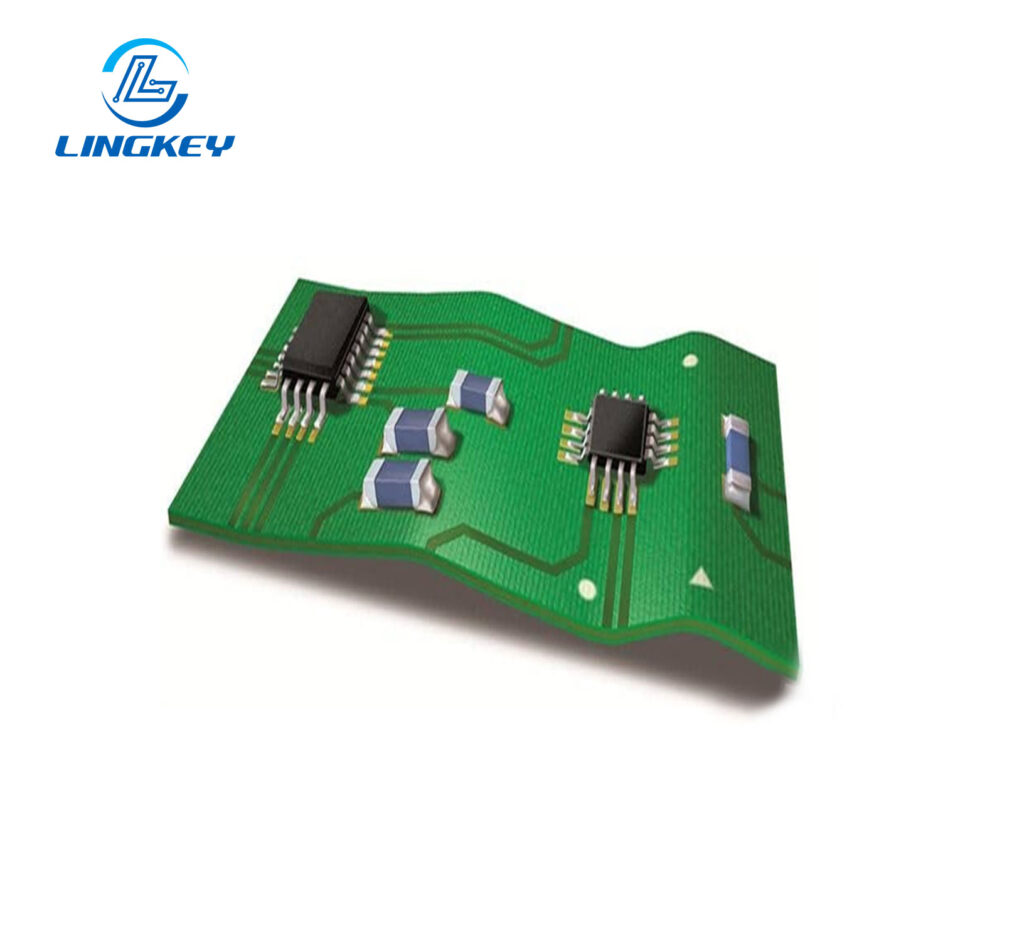
PCB warpage is when the PCB bends, bows, or twists from its target flatness Warping and bowing of PCBs is common and sometimes acceptable. It often appears with the edges or corners of the board lifting up from a flat surface, which affects its ability to mount components accurately and to run reliably. The warpage of a PCB may occur at various process steps of PCB fabrication, component mounting, or even storage, particularly when thermal stress, mechanical stress, or moisture absorption are applied.
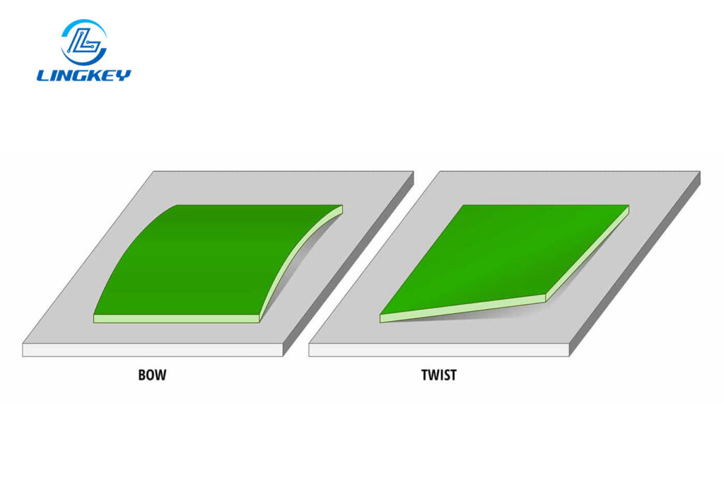
Typical manifestations of PCB warpage include:
- Bowing:The board curves lengthwise.
- Twisting:The board’s corners lift in opposite directions.
- Camber:Board edges are not straight.
PCB bending is particularly important in Surface Mount Technology (SMT), as small distortions may lead to bad component placement and poor solder joints.
PCB Warpage Standards & Measurement Criteria
The flatness of the PCB needs to be controlled to achieve good assembly and soldering results. International standards like IPC-A-600 and IPC-TM-650 provide limits for allowable PCB warpage.
IPC Standard Warpage Limits
PCB Type | Max Allowed Warpage (as % of diagonal) |
SMT (Surface Mount) | ≤ 0.75% |
Through-hole mounted or unmounted | ≤ 1.5% |
High-Precision Assembly | ≤ 0.5% or ≤ 0.3% |
Warpage Measurement Methods:
- Place PCB on a flat surface, use a feeler gauge to check gaps.
- Use a dial indicatorfor localized height measurements.
- Employ 3D scannersor Coordinate Measuring Machines (CMM) for high-precision, full-surface profiling.
- IPC-TM-650 details standard measurement procedures for uniformity.
Causes of PCB Warpage
PCB warpage is result of a combination of multiple factors that includes design, materials, processes and handling.
Material-Related Factors
- Substrate Choice:Fiberglass-reinforced FR-4 or polyimide materials have the different thermal expansion coefficients (CTE).
- Material Imbalance:Copper and dielectric layers have to uniformly expand and contract when being heated/cooled in the reflow oven; mismatch causes the board to bow.
- Material Thickness:Thinner PCBs are far more prone to warping.
- Moisture Absorption:FR-4 or other substrates absorbing water can swell and contract unevenly.
Manufacturing Process Factors
- Lamination Process:Thermal stress during pressing can “set” a board’s bow or twist if pressure/temperature is uneven.
- Copper Clad Boards:Uneven copper distribution during initial board pressing causes stress imbalances.
- Solder Mask/Silkscreen Baking:Non-uniform heating can warp areas of the board.
- Cooling and Heating Cycles:Rapid temperature transitions, especially repeated during thermal cycling, cause fluctuating expansions and contractions.
Engineering Design Issues
- Copper Layout:Uneven copper areas create copper surface tension and the board is bowed when heated.
- Stackup Asymmetry:Uneven number of prepregs or poor layer balance increases the risk for warping.
- V-Cut Design:Deep or incorrect V-cuts can compromise the stability of the structure, causing the boards to be more flexible and to bow during assembly.
Storage and Handling Issues
- Improper Storage:Stacking or storage under an uneven load, especially with thin PCBs, leads to bending.
- Environmental Exposure:High humidity or temperature cycles in storage areas can warp PCBs before use.
- Component Placement:Heavy components on one side of the board may exert stress on the board and cause it to bend during soldering.
Effects & Risks of PCB Warpage on Assembly and Performance
Impact on Automated Assembly Line
- Pick and Place Accuracy: Warped boards don’t sit properly, causing misplacement or failed pickup of SMT components.
- Solder Paste Printing Issues: Board distortion leads to inconsistent paste thickness, causing solder bridges or gaps.
- Reflow Soldering Defects: While heating, warpage leads to movement—SMT components can “tombstone,” tilt, and occasionally break free while soldering.
- Machine Placement Errors: Automat-equipment tuned for flat PCBs measures heights falsely, which also leads to assembly defects.
Impact on Product Performance & Reliability
- Bad Solder Joints:Irregular contact and bonding due to misalignment.
- Tombstoning and Misalignment:Small parts, such as chip resistors, often fail to solder flat, rising up on one side.
- Connectivity Problems:Unreliable connections, causing intermittent faults.
- Stress on Assembly:Warped boards, when forcibly fit into enclosures, may crack internally or stress solder joints over time.
- Product Delays & Recall:Yield loss due to failures in PCB reliability testing or AOI (Automated Optical Inspection) during production.
Table: Common Assembly Risks with Warped PCBs
Assembly Process | Effects of Warpage |
Pick and Place | Poor component alignment, rejected placements |
Solder Paste Printing | Inconsistent stencil contact, excess/insufficient paste |
Reflow Soldering | Shifting component positions, poor solder joint formation |
Wave Soldering | Open solder joints, bridging, uneven solder fillet |
Test and Inspection | False defects, poor test contact, misread errors |
How to Check and Characterize PCB Warpage
Visual Inspection
- Place the PCB on a certified flat reference table. Look for visible gaps at the corners or edges.
- Use a feeler gaugeto measure any lift above the surface.
Mechanical Devices
- Use a dial indicatorat critical points to quantify height deviations across the board.
- For high-precision applications, use warpage fixturesor flatness jigs for reproducibility.
Advanced Tools
- 3D scannersand CMMs provide detailed surface profiles, ideal for high-density PCB stack-up
- Thermal imaginghighlights areas of uneven thermal expansion during and after soldering and reflow processes, often revealing warpage problems before they lead to assembly defects.
Standard Methodologies
- Follow IPC-TM-650for standardized warpage testing. This internationally recognized standard details accurate measurement procedures to ensure consistency and comparability.
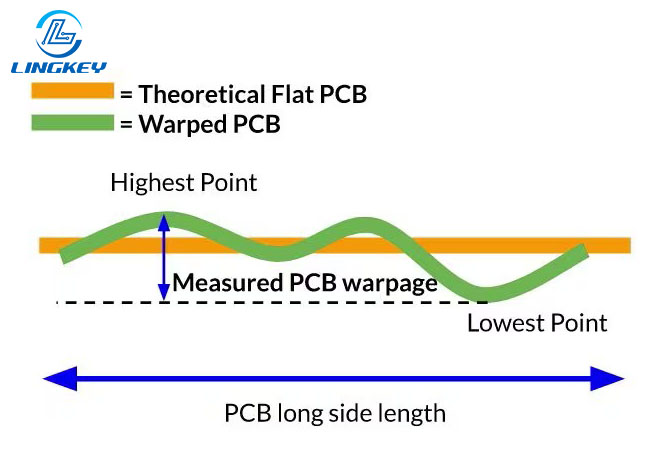
- Measurement is usually performed at the board’s worst-case diagonal to the end to capture the largest deviation from flatness.
- Warpage is calculated using the formula: Warp (%) = (Maximum Deviation from Flatness / Diagonal Length) x 100
PCB Warpage During Processing – Key Causes
Even with the best materials and designs, PCB warpage can occur during processing stages if careful controls are not in place.
- Weight of the Circuit Board:Larger or thicker boards are of course more prone to warping, particularly when exposed to high temperature gradients in the reflow oven or wave solder bath.
- V-Cut Effect:Deep or eccentric V-cuts generate stress concentration and make the PCB susceptible to bending, especially after panelization.
- Lamination and Pressing Process:Thermal and pressure symmetry should be observed in the PCB pressing process. Any unevenness induces internal stress which will lead to warpage after cooling.
- Solder Mask and Silkscreen Baking:Inadequate baking parameters (time, temperature) or non-uniform heating can warp sections of the board, especially if copper distribution is uneven.
- Heating and Cooling Cycles:Boards undergoing sudden changes from hot to cold (like in reflow ovens and soldering) expand and contract at differing rates causing a thermal imbalance and subsequent warpage.
Prevention and Minimization of PCB Warpage
Preventing warping of PCBs is much simpler and more cost-effective than repairing them later. Below are key methods to reduce PCB warpage throughout the design, manufacturing, and storage:
PCB Design Best Practices
- Balanced Stackup:Ensure symmetry in copper distribution and layer count. Any imbalance increases the likelihood of board warping.
- Optimized Copper Layout:Distribute copper features as evenly as possible on both sides to prevent thermal gradients and tension.
- Board Structure:Use standard sizes and avoid excessive board length/width that increase the risk of bending.
- Choose High-Tg or Low-CTE Materials:Especially for high-temperature or high-density boards.
Manufacturing Controls
- Pre-Bake PCB:Conduct pre-baking to eliminate any residual moisture and stress, which is particularly crucial for polyimide and FR-4 substrates.
- Controlled Heating/Cooling:Gradually heat and uniformly cool boards in reflow ovens; avoid abrupt temperature changes that cause sudden thermal expansion/contraction.
- Prepreg Layer Symmetry:Align prepreg directions to match core layers, maintaining structural integrity during lamination.
- V-Cut Design Optimization:Ensure V-cuts are shallow and correctly placed.
Handling & Storage
- Support During Storage:Use flat fixtures to support boards; avoid stacking boards with heavy weights or in environments prone to high humidity and temperature fluctuations.
- Vacuum Sealed Packaging:For sensitive or high-value boards, vacuum sealing prevents moisture absorption and physical stress during storage and transportation.
- Proper Shelf Practices:Never leave boards “leaning” vertically or pressed unevenly on racks.
Table: Top Prevention Measures
Step | Description |
Material Selection | FR-4, polyimide; high-Tg, low-CTE |
Balanced Layout | Even copper and layer symmetry |
Pre-baking | Moisture removal/thermal stress relief |
Controlled Processing | Uniform reflow, lamination, and cooling |
Intelligent Storage | Flat fixtures, no stacking, vacuum sealing |
Design Simplicity | Avoid excess panelization, complexity, unsupported areas |
Solutions and Repair Methods for PCB Warpage
When distortion is found after the processing steps or in the process of assembly, certain corrective actions can be taken, but prevention is the best cure:
PCB Bow and Warp Repair in Manufacturing
- Roll Leveling:Mechanically passing the warped PCB through rollers can reduce modest bows, especially for thin or large boards.
- Cold Press Leveling:Placing the PCB under a press at room temperature helps flatten mild warps.
- Hot Press Leveling:Similar to cold pressing but utilizing gentle heat to help re-form the PCB, particularly where polymers allow some re-flow or stress relief.
- Bow Mold Method:Using specialized jigs, the PCB is held in a flat position while being heated gently, “resetting” its flatness.
Reinforcement and Structural Solutions
- Reinforce the Board:Add internal or external mechanical supports at support areas or across the PCB surface for critical assemblies.
- Surface Bonding Technology:Apply bonding agents or adhesives at strategic points to maintain flatness where minor distortion is discovered.
Characterizing PCB Warpage
Measurement, recording, and analysis of warpage are essential for process enhancement and continuous quality assurance.
Key methods:
- Dimensional Reporting:Log measurements from flatness checks (dial indicators, feeler gauges, 3D scanners) alongside PCB batch numbers for traceability.
- IPC Testing Standards Compliance:Routinely test with reference to IPC-TM-650 or other relevant standards.
- Trend Analysis:Use statistical tracking to spot patterns and recurring issues in PCB warpage measurement—sometimes a change in supplier, storage, or lamination can spark new issues.
Frequently Asked Questions About PCB Warpage
What is the acceptable PCB warpage according to IPC standards?
Can PCB warpage be repaired after assembly?
Is flexible PCB more prone to warping?
How often should warpage be checked in manufacturing?
What is “tombstoning” and how is it related to warpage?
Conclusion
PCB warping is a multifaceted problem that influences the assembly accuracy, solder joint integrity, yield, and reliability of the product over time. Prevention is a proactive measure and can be accomplished with good PCB design considerations, appropriate material selection, well-managed manufacturing processes and disciplined handling and storage throughout the life of the product. You can also minimize warpage by working with a knowledgeable PCB manufacturer like LingKey who will optimize stack-up design, enforce process control, and manage quality that meets or exceeds IPC standards. With LingKey’s high-density/high-reliability PCB expertise, your design will be proven productive with consistent flatness, stable assembly, and reliable end-product quality from prototyping to mass production.
")
")


")
")
")


