PCB Test: Best Practices, Testing Methods, and the Role of Test Fixtures in PCB Testing
Introduction to PCB Testing and PCB Test Fixtures
PCB testing is the demand of electronics industry as the complexity of the PCB and precision of PCB products are increasing year by year. PCB testing ensures that every PCB works as it should before being assembled into end products. The significance of PCB testing is quiet and it can’t be ignored with the increase of complicated PCB design in nowadays devices.
The PCB test fixture used in circuit testing enables efficient, repeatable and reliable testing by making contact with the PCB at specific test points. These test fixtures allow for high-performance testing by positioning test probes so that they physically contact the test points on the pcb, enabling precision and repeatability when testing placement of components, circuit continuity and overall pcb functions.
Integrating test fixtures into the design and production process satisfies the individual testing demands and also helps keep up with international test standards for pcb assembly testing.
Why Thorough PCB Testing Matters
Testing PCBs is more than just a basic continuity check, the testing must be thorough to ensure quality and meet regulatory standards. Intensive testing for early fault detection reduces both test time and cost and also avoids very expensive field faults. The well-planned tests at all levels reveal net routing errors, faulty vias or contamination when the PCB is exposed.
The results from each type of test, whether stress testing, burn-in, or contamination testing, are recorded as test data which allows the manufacturer to perform trend analysis, production test process optimization, and evolution of the testing requirements on future projects.
Testing has also a strategic importance to be used to prove the conformity to the standards of the types (IPC-6012, IPC-A-600), and to ensure to your customers that your products exceed those of your competitors in reliability and life.
Why So Many Different PCB Tests?
With various PCB layouts and complexities, each test method simulates different faults on a PCB that may be found in the field. Board test methods are specialized: bare board test is concerned with opens and shorts whereas in-circuit test (ICT test probes) is concerned with component values and presence. Environmental and burn-in tests stress the PCB to prove it can survive in a hostile environment.
Typical PCB Testing Workflow (with Test Fixtures)
| Testing Phase | Type of Fixture/Equipment | Aspect of PCB Design or Function Tested |
| Bare Board Testing | Flying Probe, Electrical Tester | Net routing, opens/shorts, pad viability |
| SPI (Solder Paste) | 3D SPI Systems | Solder pad coverage, deposit volume |
| AOI (Optical) | Optical Fixture, AOI Machine | Component misalignment, missing parts |
| X-Ray | X-Ray Fixture, AXI System | Hidden joints, solder under BGAs |
| In-Circuit Testing | Bed of Nails Fixture, ICT Probes | Pin-to-mesh component presence, electrical paths |
| Functional Testing | Custom or Hybrid Fixture | Circuit operation under working conditions |
| Burn-In/Stress Test | Environmental/Custom Fixture | Product reliability, early failure screening |
Types of PCB Tests and Corresponding Test Fixtures
The need for testing is highly influenced by the PCB complexity and the production quantity. Let’s start by discussing the main types of test fixtures and how they fit into the testing process.
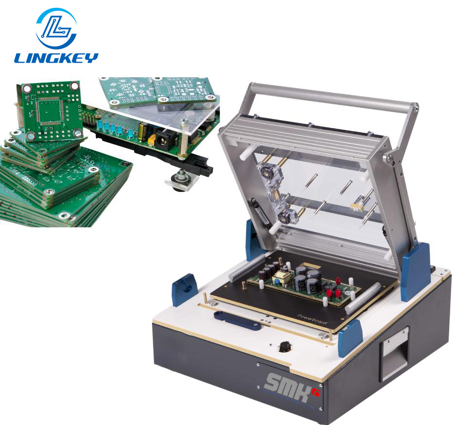
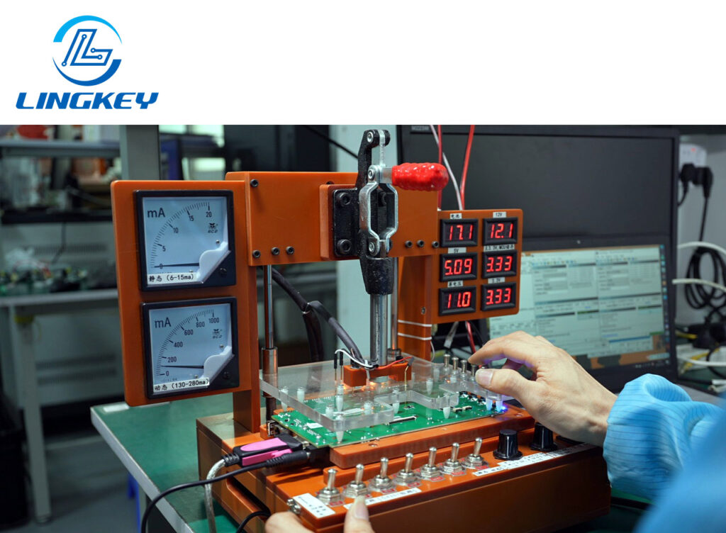
In-Circuit Testing (ICT) & Bed of Nails Test Fixture
In-circuit testing (ICT) involves the connection to the test points on the PCB under test through an array of ICT probes (spring-loaded pogo pins) by using a bed of nails PCB test fixture. This allows for quick, precise, and automated circuit testing, making it essential for high-volume production testing.
- Advantages:High-speed testing, full coverage and good repeatability for standard PCBs.
- Ideal for:Stable layouts of complex PCB assemblies numbering many pieces.
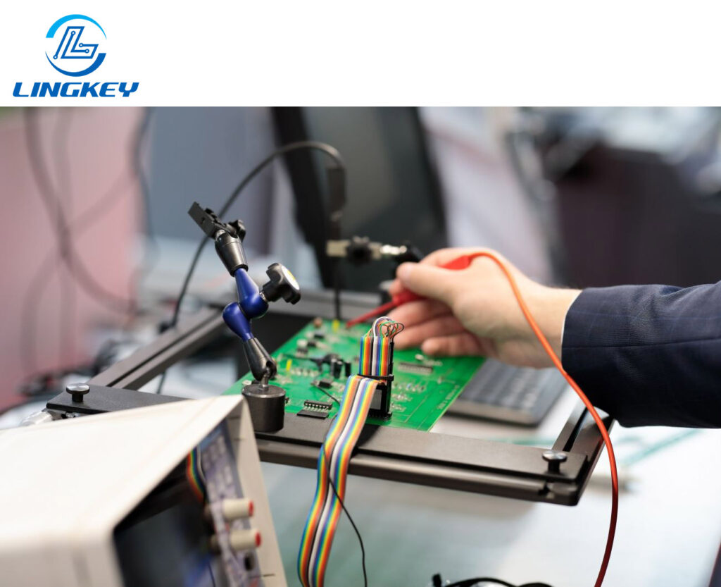
Functional Test Fixture
Functional testing is a testing process that checks if a PCB board performs as it should in the real environment. Today, a functional test fixture is typically customized for the specific PCB design and application, particularly when testing PCB functions such as communication protocols or power delivery.
Flying Probe Test Fixture
The flying probe test fixture is suitable for prototype development, small-batch production and where test point access has to be flexible due to frequent design changes. This method of testing eliminates the cost of fixture builds and enables quick modifications for evolving testing methodologies.
Combination Fixtures
Combined test fixtures are a combination of multiple test probes and test stages (i.e: in-circuit and functional test) implemented in a single fixture to increase throughput and better fault coverage especially for complex PCBAs.
Custom Test Fixtures
For the complex PCB layouts with nonconventional footprints or special testing for application-specific issues, a custom test fixture is designed. Custom fixtures can take the form of environmental chambers for burn-in testing, or complex actuation mechanisms that hold the non-standard board.
Must-Know PCB Testing Methods
The PCB test strategy is customized for the needs of the board and the production. Methods of PCB testing are functional testing, in-circuit testing, optical inspection and many more.
Key Methods:
- Bare Board Electrical Testing:Checks net routing, opens, and shorts before assembly.
- Solder Paste Inspection (SPI):Ensures proper solder coverage to avoid board failures.
- Automated Optical Inspection (AOI):Checks component placement and solder joint quality with high-resolution camera.
- X-Ray Inspection:Critical for densely packed PCBs, reveals hidden solder and allows contamination testing.
- In-Circuit Testing (ICT):Uses standard ICT probes for rapid, automated probing of circuit location, component values and network integrity.
- Functional Testing (FCT):Runs the PCB under normal operating conditions for a full evaluation.
- Burn-In Testing:Such a stress test subjects the PCB to elevated temperature and voltage for an extended period of time, allowing it to detect premature failures due to weak
Common PCB Defects and How to Catch Them Early
Efficient testing minimizes circulation of boards with:
- Opens/Shorts:Regular electrical testing directly on points on the PCB can catch these.
- Component misplacement or absence
- Cold solder joints & solder bridges
- Contaminationfrom dust, flux, or residuals is often uncovered by AOI, X-ray, or dedicated contamination testing.
- Insufficient solder:Detected through AOI and SPI systems.
- Degraded signal transmission:Results in failed board under PCB functional testing.
Top Failure Checklist:
- Opens & shorts
- Solder bridges
- Faulty vias
- Incorrect component polarity
- Incomplete net routing
- Lifted pads/traces
- Improper solder mask application
- Physical contamination
Key Components of a PCB Test Fixture
The precision and stability of the connection to the test points is what keeps the test system stable during production. A standard pcb test fixture consists of:
- Base and Frame:Provides rigid support for accurate alignment.
- Test Probes (Pogo Pins):Provide access to test points on the PCB (e.g., edge connectors, vias, and component pads).
- Actuation System:Reliable and consistent probe pressing for fast and accurate test results.
- Mechanical Alignment Guides:Maintain position, crucial for tight PCB layouts and high probe counts.
- Control Electronics:Interface with ATE and manage test data
- Safety Features:Guard against ESD and operator errors.
PCB Test Fixture Design Considerations
PCB layout for test and fixtureability is an important part of the design and the manufacturing process the entire. Proper PCB design allows better test point access, makes testing easier and reduces fixture complexity, thus increasing the overall test process efficiency and cost reduction.
Core Considerations in PCB Test Fixture Design
Access to Test Points: The layout should be optimized for easy access to t est probes for testing, using dedicated pads, vias or exposed copper. For the high speed PCB and complex PCB design, considering accessibility at the beginning will save much cost. By hard-to-reach test points, testing can be limited in depth and rigor, and on some boards some tests even can be made impossible.
Testing Requirements: Specify testing needs in advance (for example, functions, voltages or protocols you want to test). A fixture should cover all points on the PCB that needs to be validated, including power rails, digital IOs and delicate analog nets.
PCB Layout and Fixture Compatibility: Think about the part of PCB design that covers fixture mounting—like providing adequate room for fixture guides, clamps, or slots. On complex PCBs, do not put vulnerable components near the fixture edges or beneath test probes, as they can be inadvertently damaged while actuating.
Type of Testing: Match the fixture design to the test type—ICT, functional, burn-in, or stress test—and the complexity of the PCB. For complex testing methods or high-speed boards, signal integrity and controlled impedance traces are a must.
Test Probes & Probe Types: Select probes to test the tip geometry needed (flat, pointed, crown), number of test cycles and the capacity of current. High-density boards may require custom arrays or micro-probes.
Mechanical and Electrical Integrity: Robust actuation design and mechanical alignment minimize setup time, provide consistent test results and prevent fixture and PCB damage. Incorporate ESD shielding and grounding for accurate, reliable test.
Data Integration: The test fixture should be transparent in supplying test data to your tracking and quality systems to enable real-time monitoring of yields, analysis of failures, and process improvement.
In realistic production settings, testability design is accomplished through the cooperation of PCB engineers and fixture designers.
During the early stage of the PCB design, the LingKey enables the customers to have DFT (Design for Test) suggestions, to optimize the test point locations, fixture compatibilities and the testing efficiency. Early partnership could also reduce fixture complexity and long-term production costs.
PCB Test Fixture Best Practices for Efficiency & Quality
Optimization of testing for speed and statistical quality is essential to maintaining quality and profit margins in today’s PCB fabrication industry.
Best Practices Include:
Incorporate Test Access Early: The inclusion of test point access early in the PCB design minimizes rework and simplifies testing, reducing the cost of the test fixture.
Standardize Test Procedures: Use established standards for the testing of PCBs and uniform methods so that the tests are valid for any type of board.
Routine Maintenance: Keep test probes clean and tightly mechanically toleranced, and electronics calibrated for accurate test. This is especially important in production testing as test speed and throughput are the most important considerations.
Documentation: Keep complete records of test jigs, processes, and results for future board versions and quality control audits.
Operator Training: Expert staff can reduce wear on fixtures, accurately process intricate PCB assemblies and detect problems at the PCB or testpoint contact or engagement early.
Design for Future Upgrades: Enable modularity or flexible probe arrays to be adjusted for new revisions or other kinds of PCBs, without requiring rework of the entire fixture.
In-House vs. Outsourced PCB Testing
Choosing between in-house and outsourced testing is a key testing-based business decision.
In-house Testing: Provides maximum control of particular test requirements, IP security, and real-time response to PCB assembly test problems. It is suitable for running standard PCB models or when frequent design changes keep outsourcing is not practical.
Outsourced Testing: Provides cost reductions for small batches or when specialized, advanced test methods are needed. Top test houses have the most modern equipment for PCB testing and are well positioned to cover a wide range of board test methods and stringent testing routines.
| Scenario | Recommended Approach |
| High-volume, recurring | In-house with dedicated fixtures |
| Prototypes, NPI, R&D | Outsource for flexibility |
| Specialized or advanced testing | Outsource unless in-house expertise is available |
For those companies that want to strike a balance between cost-optimized and advanced test solution, a collaboration with a well-established manufacturing-test service provider is often the right way to go.
LingKey provides one-stop solutions for PCB fabrication and test fixture, serving customers from prototype validation through mass production while maintaining full compliance with global IPC standards.
PCB Test Fixture Maintenance and Troubleshooting
Regular upkeep is essential for testing to ensure fixture performance doesn’t degrade over time:
Visual and Electrical Inspections: Inspect for bent pins, fatigued springs, or debris – especially if you are regularly touching the PCB.
Cleaning Routines: Use alcohol or designated cleaners to prevent the test probes, sockets, and guides from accumulating residue or debris that can lead to erroneous results or cause damage to the surfaces of the boards.
Calibration: Regularly calibrate the electrical portion of the fixture and the ATE interface to ensure that the test results are representative of the real board performance.
Troubleshooting: Use a known good standard board that passes all tests to check the fixture to isolate board faults versus fixture issues.
Good fixtures increase yield and make long term maintenance easier.
Since the structure of the fixture at LingKey is designed to be robust, repeatable and allow for easy replacement of probes, manufactures are able to keep consistent testing performance throughout their product life.
Cost Expectations for PCB Test Fixtures
Testing time and expenses vary on complexity of fixture, type of test, and level of automation.
- Bed of Nails Fixtures:$3,000 – $20,000 (high complexity, best for high-volume testing)
- Flying Probe Fixtures:$1,000 – $5,000 (lower upfront, flexible, suited to prototype/testing without large runs)
- Functional Fixtures:$2,000 – $10,000+ (custom features, high accuracy)
- Custom Fixtures for Complex PCB Designs:$5,000 – $40,000+ (fully tailored to advanced/complexity of the PCB)
Cost can be saved by making the PCB design for test, by standardizing the test point locations, and utilizing modular fixture solutions that can be modified for various PCB types.
Industry Standards & Compliance
Adherence to industry-standard test procedures such as IPC-6012 and IPC-A-600 is required. These standards provide minimum process control, PCB fabrication integrity and board testing method effectiveness levels.
- IPC-6012sets requirements on materials, fabrication, and electrical attributes.
- IPC-A-600clearly lays out inspection techniques, acceptance conditions, and quality thresholds for both standard and complex boards.
Compliance guaranteed consistent, accurate testing and business with clients who demand global certifications.
2026 Trends in PCB Testing & Test Fixtures
The landscape for testing PCBs is rapidly evolving:
AI-Driven Inspection: AI-based optical and X-ray inspection allows for more rapid and precise outcomes, transforming the domain of contamination testing and failure analysis.
Integrated Smart Fixtures: IoT connectivity powers the real-time test data feedback, predictive maintenance, and enhanced visibility across the diversified lines.
Advanced Testing Techniques: High-frequency circuit boards and small form factor devices lead to investments in new probe technologies, precision alignment, and AI-based analysis.
Environmental and Burn-In Testing Automation: Contemporary PCB manufacturers employ automated burn-in test cycles to capture failures that were not detected in the quick functional tests.
Conclusion and Recommendations
Testing is an integral part of PCB design and production. The rapidly growing complexity of PCBs and stringent quality demands make full and accurate testing at all production stages a must. The selection of the appropriate test fixtures guarantees a robust, fast and dependable testing, protecting the end-user satisfaction and the image of the company.
To recap:
- Design the PCB for testability: Strategic placement of test points, considering fixture compatibility.
- Select the right type of test fixture: Scale with production needs, PCB complexity, and type of testing required.
- Maintain rigorous testing standards: Frequent calibration, following IPC standards, and ongoing enhancement of board testing
- Leverage test data: For predictive maintenance and ongoing process optimization.
- Adopt cutting-edge solutions: AI-driven inspection and smart fixtures for future-proof quality control.
Testing for speed, accuracy and repeatability turns pcb manufacturing into a quality-led, cost-effective process which results in it not only meeting customer expectations but more often exceeding them with appreciative customer feedback and repeat business.
For professional advice or personal pricing on PCB test fixtures, please contact the engineering team at LingKey. With deep PCB manufacturing knowledge and test integration expertise LingKey enables the creation of cost effective, high yield, and scalable testing solutions that are optimized to their customer’s production requirements.


")

")
")

