Understanding PCB Warpage: Standards, Causes, Measurement, and Prevention
Introduction to PCB Warpage
In the world of high-end PCB assembly, warpage is a typical, yet very annoying problem encountered in the process of fabrication and assembly. PCB warpage is the unwanted distortion – bending or twisting – of a PCB away from its designed flatness. Knowing the sources of warpage and the best warpage prevention techniques is essential for having a dependable assembly, achieving good signal integrity, and maintaining the quality and reliability of the electronic products in general. Due to increasing complexity of modern PCB designs, even small amounts of warpage can cause assembly failure, poor electrical connection and reduced assembly yield.
What is PCB Warpage? (Definition & Basics)
Warping in PCB assembly is when a board bends or twists away from its original flat plane over the length of its surface, causing the PCB to bend or twist. Whether the warpage is bowing, twisting, or a combination of both, it creates difficulties for manual and robotic assembly. This distortion is frequently caused by a number of different factors that lead to PCBs becoming warped during assembly or storage.
Key Factors in PCB Warpage
- Materials in PCB Fabrication: The industry standard laminate, FR-4, is hygroscopic and has a differing coefficient of thermal expansion (CTE) from copper and prepreg, resulting in internal stress during processing.
- Assembly Process: The PCB can be distorted by the stress of manufacture and uneven copper distribution, and this is exacerbated by repetitively heating and cooling.
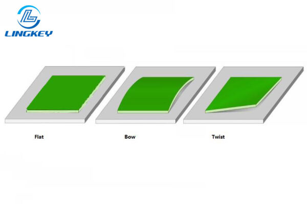
Types of PCB Warpage
- Bow(uniform bending across its surface)
- Twist(corners not co-planar, often seen in multilayer PCBs)
- Complex(combination of bow/twist due to uneven internal stress)
To understand pcb warpage it is necessary to know basic how pcb materials, process steps and post processing practices can cause bending or twisting.
PCB Warpage Standards and Allowable Limits
Meeting IPC standards is a must for quality and dependable assembly.The permissible warpage (WD) is commonly specified as a percent of the diagonal length of the board:
| Application | Max Allowable Warpage | Reference Standard |
| General Electronics | 0.75%–1% | IPC-A-600 |
| Automotive Electronics | ≤0.7% | Stricter Requirements |
| Aerospace Electronics | ≤0.3% | Highest Reliability |
PCB warpage wreaks havoc on industries such as optical, automotive, and aerospace where the warpage tolerances are even more stringent. Warpage was accurately measured using standards, so that the failure of assembly resulting from a problem of fit or connection can be greatly reduced.
How to Check and Measure PCB Warpage
Visual and Instrumental Measurement
- Lay the PCB on a reference flat plate and adopt a laser scanning system or mechanical jig to measure the warpage over its surface.
- Automated Optical Inspection (AOI) can discover warpage problems while or after assembly.
- Employ dial indicators, flatness gauges, or cutting-edge laser scanning for ultra precise measurements.
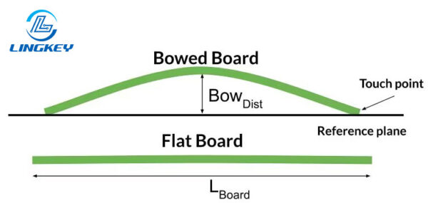
IPC-TM-650 Measurement Method
Measure the height deviation maximum at the set of points on the entire surface of the board and compare this value with the length of the diagonal of the board for the conformance with the IPC standards.
Calculation Formula
Warpage (%) = (Maximum Height Deviation ÷ Board’s Diagonal Length) × 100%
Warpage measurement, panelization design, proper fixture and warpage monitoring will contribute to maintain flatness and control of warpage during the process of PCB assembly.
Top Causes of Warpage in PCB Assembly
Knowing What Causes PCB Warpage Enables You to Optimize your design and assembly process for less assembly failures.
PCB Warpage Causes and Contributing Factors
- Different Coefficients of Thermal Expansion: Variations between layers during heating/cooling.
- Material Mismatch and Improper Material Selection: For example, using fr-4with moisture absorption or low-quality laminate.
- Uneven Copper Distribution: Heavy copper pour on one side or layer leads to pulling and bending.
- Stackup Asymmetry: Unbalanced stackups cause residual stress and warpage during assembly.
- Soldering Process Stresses: Aggressive reflow profiles and wave soldering introduce thermal shock.
- V-Cut Design and Panelization: Deep or inconsistent V-cuts make PCBs more prone to warpage.
- Dummy Copper Fills: Can help balance copper but may also cause issues if poorly implemented.
- Storage Conditions: Humidity and poor stacking cause warpage even post-fabrication.
- Mechanical Handling Accidents: Dropping, improper fixture use, or stacking can cause local bending or twisting.
Many factors cause the warpage risk to rise in early stage of both fabrication and assembly, and thus, the root causes of PCB warpage should be well taken consideration.
Impact of PCB Warpage on Assembly, Signal Integrity, and Reliability
Quality and Reliability Concerns
PCB warpage can prevent reliable assembly, leading to issues such as:
- Assembly Yield Drop: Lowers the number of boards meeting spec.
- Automated Assembly Errors: Automated pick-and-place machines rely on flat substrates.
- Poor Electrical Connections: Warpage results in lifted leads, resulting in open, bridged, or cold solder joints.
- Signal Integrity Degradation: Warpage can alter the trace geometry, causing impedance variation, especially in high-speed or optics related applications.
- Optical Component Misalignment: Warped PCBs in systems with optical alignment require stricter flatness.
In general, Warpage and standard compliance is the basis of high-quality and reliable electronics.
Warpage Analysis and Detection Techniques
Engineering Methods & Automated Inspection
- Laser Scanning and Optical Inspection: Rapid, precise, and suitable for both prototype and mass production.
- Finite Element Analysis: Estimate the warping risk during the design phase, especially for high density or multi-layer PCBs.
- Thermal Profiling: Analyze actual reflow profiles to detect causes of warpage in PCB assembly.
Accurate warpage analysis and understanding of stress during processing enable faster root cause investigation and higher quality optimization.
Warpage Prevention: How to Prevent and Reduce PCB Warpage
Distortion prevention begins at design and continues through assembly.Here’s how you can greatly reduce the risk:
PCB Design Optimization
- Optimize Copper Distribution: Use copper balancing and dummy copper fills.
- Panelization and V-Cut: Keep V-cuts shallow and panel sizes moderate.
- Symmetric Stackups: Even layer and material distribution resist bending forces.
- Material Selection: Choose high-quality laminate and prepreg with similar CTE.
Manufacturing Process Adjustments
- Gradual Heating and Cooling: Slow, controlled thermal ramps reduce thermal shock.
- Baking: Eliminates residual moisture.
- Accurate Fixture Use: Adequate support during reflow and transport prevents warpage during assembly.
- Quality Control Steps: Warpage measurement at multiple stages, especially before reflow.
Handling and Storage Best Practices
- Store PCBs in moisture-controlled, flat environments (avoid stacking).
- Use proper packing, anti-static bags, and support fixtures during shipping.
PCB Warpage Repair and Rework
Rework is sometimes possible for minor warpage:
- Mechanical Roll Levelers: Can gently flatten minimal bow or twist.
- Bow Mold and Controlled Baking: Carefully reheating and supporting a PCB to relieve stress.
Larger quantities, pressing slabs with special jigs under controlled heating/cooling may restore flatness. However, the rework should be done with care as new defects may be introduced, long term reliability may be compromised or signal integrity may be impaired, more so with high-density or optical PCBs.
Key Consideration: Not all bent PCBs are repairable. Warpage-induced assembly failure boards usually contain inner layers delamination or microcracks which can not be seen with naked eyes. When warpage is out of tolerance after assembly, changing the affected boards is usually the best way to maintain consistent quality and reliability.
FAQs about PCB Warpage
Q: What’s the top cause of warpage in PCB assembly? A: The principle cause is the mismatch of materials with different coefficients of thermal expansion, compounded by nonuniform copper distribution and severe thermal cycling in assembly.
Q: How does warpage affect automated PCB assembly? A: Warpage can compromise pick-and-place accuracy, induce soldering defects and cause automated optical inspection (AOI) alarms, which in turn would typically result in severe assembly yield loss.
Q: What’s the best way to measure warpage accurately? A: Use laser scanning or dial indicators along the diagonal length of the board with the PCB secured in a precision fixture. Always consult IPC standards for method and allowable limits.
Q: Can I prevent PCB warpage through design alone? A: You can mitigate risk substantially with good copper balancing, symmetrical stackups, proper panelization, and intelligent material selection. However, the fabrication and assembly process control are also important for overall warpage prevention.
Q: Does even minor warpage matter? A: Yes. Even slight variation may introduce placement or soldering defects in the tight-tolerance, high-quality PCB assemblyprocess, especially for fine-pitch or optical parts.
Advanced Warpage Issues in Multilayer and Optical PCBs
The distortion problems are exacerbated when multilayer, HDI, or optical PWB’s are involved. With more layers and connections, there are more interfaces between materials with different thermal expansion coefficients. This makes it more likely to get stressed in manufacturing and possibly bowing or twisting become more severe. In these complex designs, engineering simulation and process control are more advanced and tighter.
Signal Integrity and Optical Alignment
The PCBs for high speed and optical applications (e.g. telecom or lidar) are the most vulnerable. Distortion can alter the length and alignment of signal paths, leading to loss of SI and optical misfires. So ensuring flatness is both good robust assembly and good device performance.
Using Simulation and Predictive Tools
Using finite element analysis and simulation allows for early prediction and mitigation of warpage risks – prior to their impact on PCB warpage in assembly. This pre-emptive move is priceless for complex, high-value assemblies.
Conclusion
PCB warping is still one of the half a dozen major problems in today’s PCB manufacturing and assembly. The combination of material, laminate properties, panelization, copper distribution, and process parameters results in countless possibilities for warpage to evolve – from the underlying causes of PCB warpage in fabrication through to warpage in assembly. Once you know the root causes of warpage, and can fold in mitigation techniques (via design optimization, better storage, more tightly controlled assembly processes, and regular warpage monitoring using state-of-the-art instrumentation), you can certainly reduce your defects, save yourself from costly rework, and produce truly high-quality, dependable electronics.
Focusing on warpage prevention and collaborating with your PCB supplier to fine tune each process step will minimize the warpage threat at an early stage and promote the flatness of the board, which in turn will maximize the assembly yield and satisfy the high requirements of the advanced electronic of today whether automotive, medical, telecom, or futuristic optical systems.
Furthermore, collaborating with a professional and experienced PCB manufacturer is crucial to controlling warpage effectively from start to finish. LingKey offers high end PCB fabrication and assembly service, with strong abilities in material selection, stackup and process control precision, assisting customers to reduce warpage risk and to maintain consistent flatness and reliability in high performance electronic applications.


")

")
")


