PCB Solder Mask: Complete Guide
Introduction
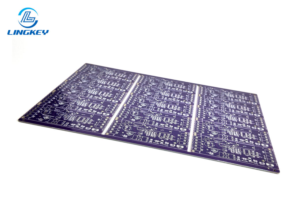
If you’ve ever looked closely at a printed circuit board (PCB), you may have asked yourself what the colorful layer on top of the PCB is — that would be the solder mask layer. This is a solder mask, a protective coating (typically green, but it could be any color) that plays a very significant part in PCB design, in the solder process and in the electronics reliability.
Benefits of using solder mask include protection of the copper in the PCB from solder bridges, corrosion and oxidation, protection from mechanical and chemical abrasion, and protection from the environment. What is solder mask and why does it matter for the PCB manufacturing process The answer is simple, strong PCB is regarded as the backbone of powerful electronics development. In this comprehensive PCB solder mask guide, you will discover various solder mask types, how to use them, their properties, and how to check that your solder mask works properly to provide you with a high-quality, long-lasting PCB.
As a professional PCB manufacturer, LingKey offers advanced-level PCB fabrication and PCB assembly service with high-quality solder mask process. With modern production facilities and quality management system, LingKey guarantees the accuracy of the solder mask, excellent insulation performance and long time reliability of the PCBs for consumer electronics, industrial equipment, automotive electronics and communication device.
What Is Solder Mask Material?
The solder mask is a specially formulated polymer layer (a solder mask ink or a solder mask film) which is applied over the copper traces of a PCB to protect them. The solder mask is a protective layer that isolates the copper circuit from the molten solder during the PCB assembly and protects the PCB from solder defects.
Purpose of a solder mask:
- Acts as a protective layeragainst corrosion and oxidation
- Prevents solder bridges and short circuits during the soldering process
- Increases long-term reliability
- Adds mechanical protection and electrical insulation to the PCB
In fact, the solder mask is the most important protective layer covered on the PCB in the PCB manufacturing process.
Composition of Solder Mask Material
The formulation of PCB solder mask material consists of multiple components which provide it the capabilities to act as a protective layer and to endure environmental and process-induced stresses:
| Component | Function |
| Base Resin | The core polymer providing adhesion, insulation, and mechanical strength |
| Curing Agent | Hardens the mask during curing, ensuring a durable shell |
| Photoinitiators | Needed for photoimageable masks—cause the mask to harden upon exposure to UV light |
| Pigments | Give distinct colors to the mask (like green solder mask, red solder mask, black solder mask) |
| Fillers & Additives | Enhance properties such as flexibility, surface insulation resistance, and chemical durability |
Solder masks are frequently classified by resin type and curing mechanism, certain formulas are adapted for high heat resistance and for fine-pitch PCB layout.
Types of Solder Mask Materials
Choosing the appropriate type of PCB solder mask is crucial for selecting the correct solder mask for your application.Here are the main choices:
Epoxy-Based Solder Mask
Epoxy is a common protective coat especially for single sided or simple PCBs. Screen printing applies the epoxy-based solder mask, which has good adhesion, but is not ideal for multilayer, high-density substrates.
Liquid Photoimageable (LPI) Solder Mask
LPI solder mask is the norm for most pcb manufacturers. This variety is applied in liquid form, exposed through a photography mask and developed under a photographic process, resulting in much more accurate openings where solder is needed (pads, vias).
Dry Film Solder Mask Material
Dry film solder mask material is made by laminating a pre-formed film onto the board, and then patterning it using photolithography. It predetermines the overall thickness, which is applied also to the high quality of PCBs and special type of PCBs requirements, like those in medics or in space.
UV-Curable Solder Mask
Fast curing under UV light, UV-curable solder mask is favorite for rapid prototyping and small production runs.
Different Solder Mask Options & Special Materials
- Polyimide for high-temperature PCBs
- Flexible PCB formulations
- Custom blends for black PCB, white, or other finishes
See solder mask on boards—each type has its own processing, performance, and cost benefits.
Colors & Finishes of PCB Solder Mask
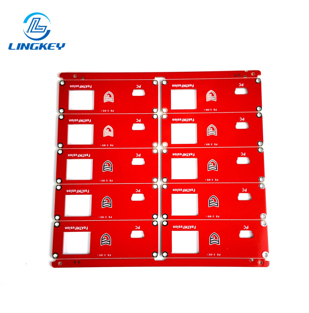
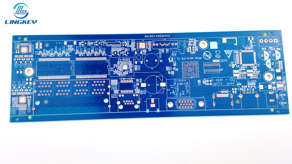
The traditional green solder mask is the most widely used in the industry, which is known for its inspection reliability and process consistency.However, other vibrant colors can be offered for special applications:
| Color | Common Application | Key Properties |
| Green Solder Mask | Standard electronics, most PCB manufacturing | Good contrast, ideal for inspection |
| Red Solder Mask | Consumer, branding, specialized products | Strong contrast, aesthetics |
| Blue Solder Mask | Medical devices, unique identification | Medium visibility |
| Black Solder Mask | High-end, luxury, black PCB variants | Conceals copper, absorbs heat |
| White Solder Mask | LED, displays, lighting electronics | Reflects light, can yellow over time |
The board color has become a factor in PCB design for the purpose of branding and inspection. But the color does not affect the fundamental protection function of the solder mask layer.
Solder Mask Properties and Performance
The properties of the solder mask affect the long-term reliability, assembly yields and the performance of the PCB.
Key Performance Indicators:
- Adhesionto the copper substrate and PCB material
- Heat resistanceduring reflow soldering cycles
- Chemical resistanceto cleaning agents, fluxes, and environmental exposures
- Surface insulation resistance(keeping signals separate even at high frequencies)
- Mechanical robustness(chipping, flexing, abrasion)
- Uniform thickness to prevent the expansion of solder mask from creating defects in high-density components
| Property | Epoxy-Based | LPI Solder Mask | Dry Film Mask | Notes |
| Adhesion | Good | Excellent | Very Good | Key for long-term PCB use |
| Heat Resistance | Moderate | Excellent | Very Good | Affects reflow soldering |
| Chemical Resistance | Good | Excellent | Excellent | Crucial for harsh environments |
| Insulation | Good | Excellent | Excellent | Impacts high-frequency boards |
| Mechanical Protection | Moderate | Excellent | Excellent | Key for mechanical safety |
Mask is a protective layer—it lives to protect and insulate the delicate copper traces for the entire lifespan of the PCB.
Functions and Benefits of PCB Solder Mask
Why is the solder mask a necessary protective layer which is required for all but the simplest of PCB designs? Here are the main functions:
- Protects against rust and oxidation of the copper, important in humid and industrial environments.
- Prevent solder bridges during manufacturing by clearly separating the soldering areas (pads, vias) with unmasked solder mask.
- Reduces risk of solder shortsin high-density or fine-pitch designs.
- Acts as an electrical insulatorand boosts the PCB’s surface insulation resistance, aiding in signal integrity.
- Provides a smooth, uniform surfacefor automated PCB assembly.
Serves as an electrical insulator and increases the surface insulation resistance of a PCB, which help in signal integrity.
Solder Mask Application Process
What is the process of solder mask application in the workflow of the PCB fabrication?Let’s dive into the step-by-step process:
1. Surface Preparation
Clean the board well to remove all dust, oil and oxidation. It is necessary for the solder mask ink / solder mask film to stick to.
2. Application
Based on the material, the mask is applied by screen printing (epoxy based), curtain/spray coating (LPI) or lamination (dry film solder mask material).
3. Patterning
For LPI and dry film types, a photography mask (also known as a phototool) is used. The board coated in the still-tacky solder mask ink or film is then registered to this mask and it is pressed into contact and only select areas such as pad openings are exposed to ultraviolet (UV) light. The UV-exposed areas of the polymer solidifies, while unexposed solder mask is still soft and is then removed The unexposed mask is softened and washed away. This is not only to make sure that the pad and via openings are formed accurately, but also to prevent the solder mask spread into areas reserved for solder.
4. Curing
Curing the remaining mask is the next step. Depending on the type of material, this can be done with thermal ovens or UV lamps. The curing solidifies the polymer, which forms a strong protective layer that can resist the high heat of the soldering process particularly during reflow and wave soldering.
5. Final Inspection and Touch-Up
The entire PCB is subjected to a thorough visual (color and clarity) and automated optical inspection (AOI) for the purpose of ensuring that the coverage is consistent, the openings are accurate and there are no defects, including but not limited to pinholes or mask misregistration. All defects found during inspection, including but not limited to coverage loss or delamination will be repaired manually to the high quality standards of PCB.
6. Marking and Finishing
The board is now ready for silkscreen (component designators, logos) and, if requested, special finishes, such as conformal coating—layering on multiple levels of protection and boosting long term PCB reliability even more.
At LingKey the Pro email mask application process conforms to the international PCB fabrication standards. State of the art coating technology apparatus, precision photolithography, and automated inspection lead to accurate solder mask openings of uniform thickness with excellent adhesion to the copper surfaces. With these production capabilities, LingKey can provide high quality PCBs for the challenging requirements of today’s electronics products.
Tips for Working with Solder Mask Material
To establish the solder mask as a real protective film during the life of the product, apply the following best practices:
- Select the appropriate solder mask material type for your PCB based on the application environment and assembly process.
- Ensure the surface is thoroughly clean prior to solder mask application to prevent poor adhesion.
- Apply appropriate exposure/curing conditions of selected ink/film to form a uniform and defect free protective layer.
- For compact layouts, work to the standards for solder mask expansion and pad clearance.
- Check the solder mask thickness at all times, variations can influence the quality of soldering and also the surface insulation resistance.
- Keep solder mask ink and film in a cool and dark place to extend shelf life and keep the chemistry is stable.
Adhering to these rules will reduce the risk of solder bridging and other assembly defects, which is essential to have to ensure a high-quality, long-life PCB.
Common Problems with Solder Mask and Prevention
Solder mask is intended to be a tough protective cover, but a break in this coverage can cause issues. Here are some common problems and their solutions:
| Problem | Root Cause | Solution |
| Peeling or lifting | Inadequate cleaning or poor adhesion | Clean thoroughly, use a compatible mask-ink or film |
| Openings too small/large | Inaccurate exposure or misalignment of photography mask | Regular calibration of manufacturing equipment |
| Air bubbles or pinholes | Entrapped air during application or fast curing | De-gas inks, apply mask in controlled environments |
| Color inconsistencies | Pigment settling or improper mixing | Mix thoroughly before use, use quality solder mask inks |
| Incomplete curing | Insufficient UV or thermal exposure | Validate curing times and lamp intensity |
Advanced Design and Special Applications
With the development of the PCB technology, the requirements for solder mask are rising. Here is how designers and producers meet a few special requirements:
Solder Mask Bridge and Solder Mask Expansion
A solder mask bridge is a thin segment of mask material between adjacent pads or traces which helps to avoid solder bridging between them. Solder mask expansion or how much larger the opening is to the pad, has to be closely controlled for high density layouts.
Paste Mask vs. Solder Mask
Don’t confuse paste mask (which defines where solder paste is deposited for SMD components) with solder mask (the protective polymer coating). They work different but are complimentary in the assembly process.
High-Frequency PCBs and Solder Mask
High-speed or high-frequency PCB signals can be influenced in their integrity by the dielectric characteristics of the solder mask. The selection of the appropriate solder mask for these designs, such as special photoimageable types, will compensate for any adverse effects.
Frequently Asked Questions
What is the main purpose of a solder mask?
The main function of the solder mask is to act as a protective layer with the influence of avoiding soldering bonding, offering the better protection from rust and oxidation and extending the life term of the PCB.
Can solder mask be applied to any type of PCB?
Yes The appropriate type of solder mask can be matched to any PCB design, from standard rigid boards to rigid-flex, flex circuits and so forth.
How does solder mask affect the soldering process?
Solder mask prevents solder defects by providing well defined pad openings and acting as a solder dam so the solder only flows on the desired locations.
Does color impact performance?
Apart from some small disparities in heat absorption (like black PCBs heating up more in reflow ovens), color mainly influences visual inspection and aesthetics, not fundamental protection.
What’s the difference between solder mask ink and film?
Solder mask is a liquid and is more suitable for LPI or epoxy masks. Solder mask film relates to dry film solder masks that are applied as a solid sheet to the pcb.
Conclusion: The Evolving Role and Importance of Solder Mask Material
When it comes to the electronics of the day, the solder mask layer is one of the crucial protective layers in the procedure of pcb fabrication. From chemical resistance and mechanical protection to electrical insulation, the correct solder mask applied correctly is essential to the maintenance of PCB reliability and, in turn, the long-term reliability of any end electronic product. Key Takeaways:
- A solder mask is a layer of coating applied over a PCB, and it is necessary to safeguard traces and increase yield.
- The correct polymer formulation—is it epoxy, LPI, or dry film—provides customized protection for your board based on its requirements.
- Contemporary PCB design, be it color or layer number, must consider the solder mask characteristics.
- For the full details on PCB solder mask, consider the application method, the end-use environment, and ongoing developments in materials technology.
The next time you see solder masks on a PCB, whether you are looking at green solder, red solder mask, black solder, or any custom color, keep this in mind: Behind every sturdy, high quality PCB lies a well-selected and optimally applied solder mask.


")

")
")


