A Brief Introduction to the Development of PCB Technology and Circuits
Introduction
The history of the PCB is one of continuous revolution, forced by need, driven by invention, and inspired by ever increasing efficiencies. From simple circuits in primitive times to today’s printed circuit boards (PCBs) utilized in electronic goods, this innovation enabled the digital age — transforming how we build, utilize and come across technology. Historicals of PCB development is beneficial for experts that have anos in the PCB field, electronic designer, and even lovers of electronics.
What Is a PCB?
A printed circuit board (PCB) is a board made of an insulating material, usually fiberglass known as FR-4, that has layers of copper board laminated together to form electrical connection paths, known as circuit patterns, to connect different electronic circuits and components. PCBs are the building blocks of computers, smartphones, car systems and medical equipment, and their dependable miniaturization and high performance make it possible to turn out product from the most basic calculator to the most sophisticated aerospace instrument.
Today, printed circuit boards are made up of layers namely signal, power, ground and special circuit pattern, all of them contributing to the strong and effective performance of today’s electronic devices. PCB Design/Manufacturing Technology: The design and manufacture of the PCB—using complex pcb layout, computers and EDA tools, and precise fabrication processes—is a basic building block of the electronics industry.
The Importance of PCB History
The PCB evolution history explains why circuit boards are the backbone of modern electronics. Tracking the progression from point-to-point wiring to its evolution into today’s HDI (High-Density Interconnect) boards illustrates the way that point-to-point wiring was supplanted by generic, dependable pcb design and production. The consequence: electronics could be made standard, scaled, and more reliable—fueling the rapid development of global technology.
By knowing the history of the printed circuit, engineers understand how each evolution of the technology such as multilayer technology or the invention of the first microprocessor, created new possibilities and new horizons for electronics design.
Early Era – From Early Wiring to Modern HDI
Before PCBs, electrical circuits were constructed using point-to-point wiring, in which each wire was hand-soldered to components. This technique was unreliable and did not scale, and the point-to-point wiring was prone to malfunction from short circuits and unreliable electrical connections. As the complexity of the electronics grew, the pressure for a better solution pushed inventors towards printing circuit connections, eventually leading to today’s highly sophisticated modern circuit boards.
The Birth and Development History of PCB Technology (1850s–1940s)
Early Innovations and Patents
The early history of pcb manufacturing started with inventions in multilayering conductors and insulators.
- German inventor Albert Hanson was the first to file a patent for a pcblike invention in 1903, leasing multi-layered conductive foils with an insulating board. Hanson’s work included ideas, which, although rudimentary, became and were essential for multi-layer PCBs.
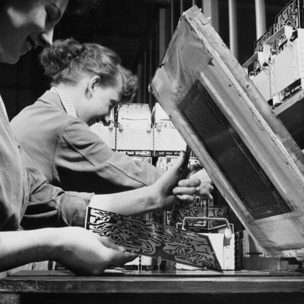
- In 1925, Charles Ducas in United States brought in the concept of printing of conductive paths on a board of insulator material with the help of stencils by using conductive ink, awarded a similar patent in 1927.
- By 1941, Paul Eisler developed the first working PCB for a radio application. The work of Eisler, particularly during the Second World War, laid down practical methods for making mass produced reliable circuit boards, which found their initial application military.
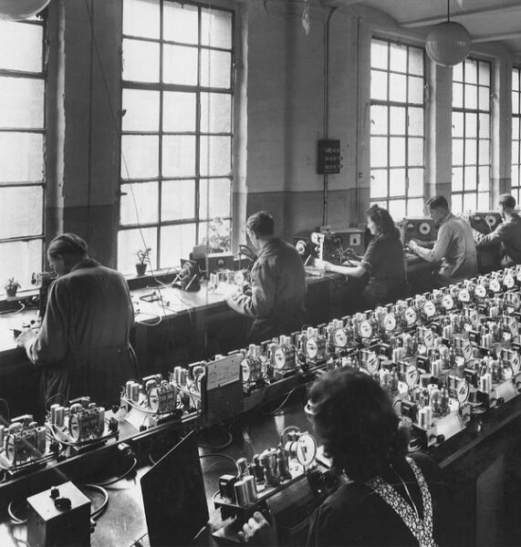
Table: Foundational Patents and Innovators
| Year | Inventor | Contribution |
| 1903 | Albert Hanson | Hanson filed the first patent for multilayer circuit patterns |
| 1927 | Charles Ducas | Introduced the first idea of printing circuit patterns |
| 1941 | Paul Eisler | Built the first functional PCB for radios |
The Industrialization of PCBs: 1950s and 1960s
As WWII came to a close, the history of the printed circuit board took another turn. The mass introduction consumer and military technologies drove standardization and process improvements.
Key Advances:
- The introduction of copper-clad insulating board and chemical etching made repetitive mass production possible.
- THT allowed for higher component density, and the addition of the solder mask layer enhanced the insulation and the robustness.
- By the late 1950s and into the 1960s, PCBs were a necessity in electronic products including transistor radios, televisions and, eventually, computers.
- In 1958, Jack Kilby of Texas Instruments developed the first integrated circuit chip. The consolidation of these ICs on PCBs created a need for tougher, denser, and more sophisticated boards, leading to the rapid development of even higher electronic circuitry.
The Digital Era: Multi-layer and Modern Printed Circuit Boards
In the 1970s and 1980s, the need for higher densities and smaller devices pushed the industry from simple single- and double-sided boards to multi-layer constructions. This makes very compact circuit boards with many copper layers, each one carefully designed in the pcb layout to prevent cross-talk, interference and to allow higher speeds.
Surface-Mount Technology (SMT) and Flexible Circuits
Surface-Mount Technology (SMT) revolutionized the PCB assembly process allowing component placement directly on the surface of the boards. It was a necessity for the miniaturization and high performance that are so common in consumer electronics.
At the same time, flexible circuit boards and flexible PCBs were introduced, using polymer-based substrates for folding and bending applications in fields including wearables, medical implants and automotive controls—leading the way for further developments in electronic design.
Modern Printed Circuit Boards and Innovations
Let’s go on a tour and discuss the cool capabilities today’s PCBs offer at every step of design and manufacturing:
- High-density interconnect (HDI) boards Trianium offers microvias formations and ultra-thin copper layers used in mobile and aerospace technologies.
- The rise of computers and EDA tool has revolutionized the pcb design. The pcb layout can now be automatically optimized for electrical, thermal, manufacturability, and reliability.
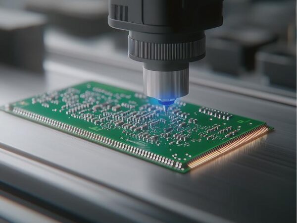
- Smart manufacturing integrates AI, automated X-ray inspection and real-time data processing to significantly reduce defects.
- Environmental practices Intectra modern circuit board RoHS compliant, lead free and produced with recyclable materials.
- Flexible circuit and rigid-flex PCB are now widely used in the industry, such as in rollable displays and mission-critical aerospace systems.
Table: Modern PCB Capabilities
| Feature | Impact |
| HDI, Multi-layer PCBs | Ultra-compact electronics |
| SMT & Automation | High-speed assembly |
| Flexible PCBs | Wearable, mobile, medical |
| Lead-Free, RoHS Compliance | Environmental safety |
| Design & Inspection Automation | Fewer defects, faster time-to-market |
Such innovations still influence the modern electronics industry where producers such as LingKey merge state-of-the-art processing technologies, intelligent automation and rigorous quality management systems to provide high-performance and dependable PCB solutions over an extensive array of applications.
Future Directions in PCB Design and Manufacturing
The progress in the history of pcb development continues with:
- 3D printed circuitsand next-gen materials for miniaturization and high performance.
- Integration of smart sensors and AI-drivenlayout tools for pcb design.
- Boards dedicated to Internet of Things (IoT), medical, and automotive fields.
- Continued efforts in green production, recycling and sustainable PCB design and manufacturing.
In the natural development of these technologies, companies like LingKey are constantly pouring resources into high-performance materials, smart manufacturing and green production to enable next-generation PCB applications in IoT, automotive and high-end electronics.
Timeline: Key Breakthroughs in the History of Printed Circuit Boards
| Year | Breakthrough/Innovator | Impact |
| 1903 | Albert Hanson filed the first patent | Foundation of multilayer PCB concept |
| 1927 | Charles Ducas, “idea of printing” | First printed wiring, precursor to actual PCBs |
| 1941 | Paul Eisler introduced the first functional PCB | Realization of the first printed circuit board, practical applications begin |
| 1950 | Mass production, copper-clad boards, THT | PCBs adopted in military, consumer goods, and industrial applications |
| 1958 | Jack Kilby at Texas Instruments | First integrated circuits on PCBs, paving the way for advanced electronic design |
| 1960 | Multilayer and flexible circuits emerge | Compact, complex boards for computers and aerospace |
| 1970 | Surface Mount Technology begins | Component miniaturization, automation in PCB layout and assembly |
| 1980 | HDI and advanced inspection introduced | Modern printed circuit boards with high-density connections, growing use of EDA |
| 1990 | Rigid-flex and highly specialized substrates | Boards for wearables, medical, and military applications |
| 2000 | Smart manufacturing, lead-free, RoHS compliance | Greener, safer design and manufacturing processes |
| 2010 | AI, IoT, real-time data in design and production | Smart PCBs powering the digital transformation |
| Present | 3D circuits, ultra-miniaturization, microvia | New types of applications, flexible pcb for next-gen electronics |
Types and Capabilities of Modern Circuit Boards
Today’s PCBs are not confined to just one configuration; circuit patterns, layers, and materials vary greatly in order to satisfy the requirements of current electronic design and products.
Key Types of PCBs
Single-Sided Circuit Boards:
- Copper traces on only one side of the insulating board.
- Common in simple electronics, LED lighting, and calculators.
Double-Sided Circuit Boards:
- Copper on both sides; allows for crossing traces and more complex circuit patterns.
- Used in militarygear, power supplies, and early computer peripherals.
Multi-layer PCBs:
- Multiple layers of copper embedded within the insulating board.
- Essential for high-speed computers, servers, and communication systems.
Flexible PCB (Flexible Circuit):
- Built on a polymer substrate for bending and folding.
- Used in mobile phones, medical devices, flexible displays, and wearable electronics.
Rigid-Flex PCB:
- Combines rigid base for mounting and flexible sections for compact assemblies.
- Ideal in aerospace technology, medical implants, and advanced automotive systems.
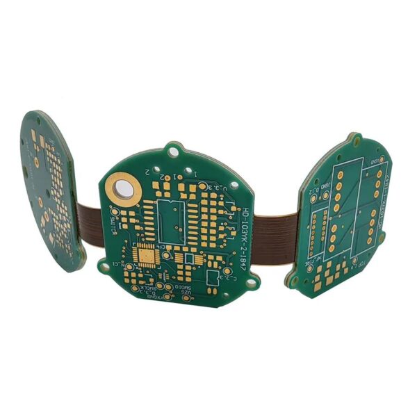
Table: Evolution of Circuit Boards
| Board Type | Decade Popularized | Key Application Areas |
| Single-sided PCB | 1950s-1960s | Radios, toys, basic electronics |
| Double-sided PCB | 1960s-1970s | Audio/video, computers, military gear |
| Multi-layer PCB | 1970s-1990s | Servers, advanced computers, telecomm |
| Flexible PCB | 1970s-1980s | Cameras, printers, medical & wearables |
| Rigid-flex PCB | 1990s-present | Aerospace, smartphones, automotive, IoT |
Frequently Asked Questions About PCB History
Q1: Who is credited with the invention of the printed circuit board?
A1: While the list of contributors is long, the German inventor Albert Hanson filed the first patent for a pcb-like insulating board in 1903. The first custom-designed, mass-producible and practical PCB was developed by Paul Eisler in 1941 for use in radios. Both are seminal in the history of the PCB.
Q2: What major changes distinguished modern printed circuit boards from early wiring?
A2: Circuit boards nowadays are complicated in their multi-layer structure, complex pcb layout for signal integrity, use of flexible substrates, and design and manufacturing automation. The original circuits were basically point-to-point wired by hand with no reliability or scalability.
Q3: How did the introduction of the first microprocessor affect PCB design?
A3: The first microprocessor needed more elaborate multi-layer PCBs. This fuelled development in EDA tools for automated pcb layout and the application of ever denser, more reliable circuit patterns.
Q4: What role did PCBs play in military and industrial electronics?
A4: PCBs were quickly adopted by the military for dependable electrical connection and miniaturization advantages. They’ve found use in systems such as military radios, guidance systems, radar systems, and space missions.
Q5: What are current trends in PCB design and manufacturing?
A5: Strong trends include the use of HDI for miniaturized electronics, smart automation, green materials, and flexible designs for IoT and medical electronics. The field is advancing toward ultra-thin, sustainable, and AI-optimized circuits.
Conclusion
The history of printed circuit boards is a journey that begins in the early days of wiring with unprocessed raw materials to modern HDI processes that enable the current era of digital and connected devices. From Albert Hanson’s original patent and Paul Eisler’s radio boards, to the multi-layer, flexible, and automated solutions utilized in computers and EDA tool today, the evolution of PCBs is peppered with moments of invention, standardization, and metamorphosis.
At each inflection point — from the introduction of the first microprocessor to the jump to flexible circuits and the adoption of green manufacturing, PCB design and fabrication have constantly moved the bar higher, making possible the today world of advanced electronics products.
Looking forward, the interplay of AI, IoT and sustainable design and manufacture will lead the next wave of PCB innovations that will evolve the breakthroughs of today into the bread and butter products of tomorrow.
In the rapidly changing electronics today, working with a professional PCB manufacturer becomes a must to turn your innovation into reliable products. LingKey offers high-end PCB fabrication and assembly services based on the state of the art manufacturing technologies and stringent quality control, enabling customers from prototyping to mass production in various applications.


")

")
")
