PCB Stencil Guide: Choosing the Best SMT Stencil, Material, and Thickness for PCB Assembly
Introduction
In electronics, the correlation of good solder paste printing and final assembly quality is unquestionable. While PCB assembly process is being optimized, the most underrated- but most vital- choice could be your choice of a PCB stencil. The optimal selection considers your PCB design, assembly requirements and manufacturing capabilities to maximize yield, control costs and provide reliable, defect-free assemblies. This all-in-one exhaustive guide is from every perspective of SMT stencil requirements, various types of stencils and essential knowledge in PCB manufacturing and PCB fabrication.
What is a PCB Stencil?
A PCB stencil (also known as solder paste stencil) is a necessary part of the SMT process that allows you to lay down the right amount of solder paste on the PCB pads so that components can be accurately placed and soldered during reflow. The openings in the stencil are aligned with the PCB design file so that the paste deposits are applied accurately.
- With today’s surface mount technology, stencils enable faster bulk production, with repeatable and reliable results in each and every printed circuit board assembly.
- In the PCB manufacturing stage, the choices and quality of your stencil define reflow defects and the efficiency of the soldering process.
- Application of solder paste is best and most repeatable if the right stencil is used which has a direct impact on the result of the reflow soldering process.
PCB assembly production makes use of precision SMT stencils at LingKey to enable consistent solder paste deposition for fine-pitch, BGA and high density PCB layouts.
What is an SMT Stencil?
Now let’s discuss the stencil, or SMT stencil—in other words, a solder stencil is a very specialized tool designed for the specifics of surface mount technology. The options for SMT stencils include simple prototypes to the complex, multi-layer or nano-coated stencil for thick stencil applications as well as for the finest pitch stencils.
SMT stencils are not the same as silkscreen during other production stages. They enable precise, consistent application of solder paste to printed circuit boards (PCBs), which is especially critical for high-volume manufacturing.
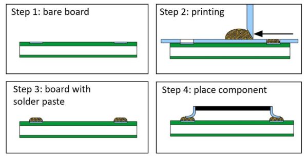
How Does a PCB Stencil Work?
The fundamental steps in the application of solder paste via a stencil include:
- Prep the Board and Stencil:Keep them clean to prevent defects during the paste printing step of the PCB assembly process.
- Secure and Align:Place the stencil (using a metal frame for rigidity) so that each opening is in perfect alignment with the PCB pads. Contemporary SMT lines frequently utilize vision systems and fiducials for this critical alignment.
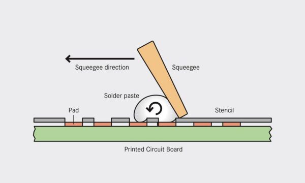
- Squeegee Solder Paste:The solder paste is pushed through the apertures by the squeegee as it moves across the stencil, leaving the correct amount of solder paste on each pad.
- Lift the stencil straight:Peel the stencil off from the PCB carefully to keep the defined solder paste deposits.
- SPI and Visual Inspection:Utilize SPI systems or magnifiers to check that each pad has an appropriate amount of paste coverage, a crucial part of dependable PCB fabrication and PCB manufacturing.
At LingKey, stencil printing quality is confirmed with SPI inspection and SMT process control to control for proper solder paste volume and establishment of assembly quality.
Types of PCB Stencils and SMT Stencils
Choosing the right SMT stencil type is critical for achieving stable solder paste printing and reliable assembly quality.
Framed (Metal Frame) Stencils
- Are the industry standard for high-volume production.
- Provide consistent tension and alignment on automated lines.
- Available in various standard sizes to fit most SMT printers.
Frameless Stencils
- Ideal for prototyping, small runs, and scenarios with frequent design changes.
- Reduce shipping and storage costs.
- Can be mounted on reusable universal frames for flexibility and cost savings.
Step/Hybrid Stencils
- Essential where you need variable paste volumes (e.g., for both fine-pitch applications and larger components in the same assembly).
- Step-down regions provide intermediate thickness for sensitive areas.
Laser-Cut Stencils
- Offer precision-cut apertures with optimal wall smoothness.
- Especially recommended for tight tolerance assemblies and fine-pitch applications.
Electroformed Stencils
- Provide unmatched aperture wall smoothness.
- Enable superior release for ultra-fine applications and advanced PCB assembly needs.
LingKey chooses different stencil solutions according to factors such as PCB complexity, component density and production volume, to ensure the best performance of the SMT assembly.
PCB Stencil Materials: Which Should You Choose?
Selecting the material is crucial to the stencil performance impacting lifetime, print consistency and uniformity, as well as compatibility to your soldering process.
- Stainless Steel:The most popular option for the majority of PCB stencils; it provides good performance at a reasonable price, particularly when it is laser-cut.
- Electroformed Nickel:Selected for demanding fine-pitch applications based on a high degree of smoothness and outstanding release of paste.
- Polymer/Mylar:Occasionally utilized for rapid prototyping, but not advised for the final product as wear is so limited.
The choice of material also affects the performance of the stencil in applications where frequent cleaning, long life, or high throughput is necessary.
PCB Stencil Thickness: The Critical Factor
The thickness of the stencil is a key factor in the quantity of solder paste deposited:
| Thickness (mm) | Application | Components Involved |
| 0.10 (thinner) | Micro-BGAs, fine-pitch, sensitive pads | CSP, QFN, 0201/01005 |
| 0.13 | Most general SMT cases (intermediate thickness) | QFP, SOIC, standard SMDs |
| 0.15–0.18+ | Thicker stencils: For large pads, through-hole, power | D-PAK, power modules, THT |
- Thicker stencils are needed for larger parts which require more solder for mechanical and electrical performance.
- Choice of thickness impacts the volume of paste and also has an effect on bridging risk and solder joint quality during PCB assembly.
PCB Stencil Aperture Design Principles
Aperture (Opening) Engineering:
The opening size and shape control how much solder is deposited.
Trapezoidal wall profiles, created by high-pressure forming (usually laser or electroformed), contribute to better solder paste release especially on fine-pitch pads.
Pad-to-aperture reduction: Most assemblies are benefited by a 5–10% shrink of the aperture with respect to the pad size, reducing the solder bridging.
Home-plate and dogbone shapes provide optimum solder flow and minimize tombstoning in resistors and small passives.
The smoothness of the aperture wall has a direct impact on the release of the paste, and this effect is more pronounced for very fine pastes as required for fine-pitch applications and high-density PCBs.
Solder Paste Compatibility with PCB Stencils
Paste particle size, rheology and type all affect suitability for your selected stencil:
Type 3, Type 4 and Type 5 solder pastes are tailored for specific aperture sizes and printing technique requirements. Type 3 is for larger apertures and standard PCBs, but it could clog or partial fill smaller stencil apertures. Type 4 has a smaller particle size allowing for better results when working with intermediate-fine-pitch components, whereas Type 5 is necessary for ultra-fine-pitch PCB design and micro-BGA assembly.
Tips for Matching Paste and Stencil:
- Use Type 3 for standard and thick stencil applications with larger components.
- Fine-pitch and high-density surface mount assemblies should choose Type 4 or Type 5 for fine-pitch/high-density, particularly with electroformed or nano-coated stencils.
- Paste compatibility should be always tested with the stencil of your choice prior to PCB manufacturing.
Solder Paste Rheology: Good rheology allows the paste to roll smoothly on the stencil, properly fills the apertures, and releases cleanly when you lift the stencil straight off the board. Rheology degradation poses a greater risk of slumping, bridging, and non-uniform solder joints during the reflow.
How to Choose the Right PCB/SMT Stencil for Your Application
Making the Right Choice for Solder Paste Application and PCB Assembly Needs:
Start with Your PCB Design File: Utilize the correct and up-to-date file output from your PCB design software of choice. Provide all paste layer details and clearly state aperture shape/size for each type of component footprint and opening.
Consider the PCB Assembly Needs and Production Scale: For prototyping and small production runs, frameless stencils or reusable frames offer flexibility and lower upfront cost. For mass production, select rigid metal frames and precision manufacturing methods that can endure multiple cycles of operation.
Match Thickness and Type to Your Application:
- Use a thicker stencil for high-current components, connectors, or through-hole technology requiring more paste.
- Select the intermediate thickness for general SMT (0.13 mm) and thin stencils (0.10 mm or below) for high density and fine pitch applications.
- For mixed components, think of a step stencil, combining zones for different height paste deposits.
Optimize for Component Mix: High density, fine pitch, and micro size components need the best stencil wall smoothness and the tight control of the aperture ratio; however, large components placed on the same PCB may require special opening shapes and the provision of more solder.
Example Table: Matching PCB Assembly Needs to Stencil Type
| Assembly Profile | Recommended Stencil Solution |
| Consumer electronics | Framed, laser-cut, 0.13 mm |
| Medical fine-pitch PCB | Electroformed nickel, nano-coated, 0.10 mm |
| Industrial with large relays | Step stencil, 0.18 mm in specific zones |
| IoT prototype board | Frameless, 0.10 mm, standard stainless |
PCB Stencil Size and Fit
Stencil size should be determined based on:
- Printed circuit board dimensions
- SMT printer/tray compatibility
- Storage and handling infrastructure (especially for framed stencils with a metal frame)
Standard Sizes: Most of the SMT production houses have a standard stencil size of either 29″x29″ or 23″x23″ for framed stencils. Frameless stencils are custom made or cut to specific job requirements, enabling you to use them for small runs or prototype assembly.
Design for Manufacturability: Stencil Considerations
PCB design plays a pivotal role in guaranteeing successful paste transfer and assembly:
- Pad Spacing and Design:Don’t cluster pads too tightly together—this is particularly crucial for fine-pitch components and when designing the stencil.
- Paste Layer Accuracy:Always review your exported PCB design files’ paste layer for completeness prior to submitting for PCB stencil manufacturing.
- Collaboration:Work closely with your assembly house and stencil supplier. Leave clear instructions for sensitive areas, step requirements or other special stencil requirements.
Step-by-Step PCB Stencil Selection Process
- Evaluate your PCB design and component mix.
- Determine PCB assembly process (manual, semi-auto, or full-auto).
- Choose framed or frameless stencils based on production volume.
- Decide on material: stainless steel stencil for most, nickel stencil for high precision.
- Select stencil thickness based on the smallest component pitch.
- Verify and optimize all openings with your supplier’s DFM review.
- Trial the stencil for actual
application of solder paste and check SPI results.
- Finalize specs for ongoing PCB fabrication or mass production.
Best Practices for Using and Maintaining PCB Stencils
- Clean after every use to avoid hardened solder paste from blocking the holes and influencing the stencil performance.
- Store stencils vertically in protective racks to avoid warpage, especially framed variants.
- Check stencil tension (for metal frame stencils) from time to time and change it when tension drops or holes are deformed.
- Set the correct squeegee parameters—rate, angle, and pressure need to be adjusted according to the type of stencil, solder paste, and PCB layout to achieve best results in the application of solder paste.
LingKey adjusts and updates the parameter of stencil printing in a continuous way while on the line during the manufacturing of SMT, which results in the best consistency of solder paste and better solder joints.
Advanced Technologies and Trends in PCB Stencils
- Nano-coatings now provide stencil life and release optimization for a more uniform soldering process, particularly in the application in fine-pitch.
- Enhanced PCB design now simulates paste deposition and recommends aperture tuning for new component layouts.
- Embedded fiducials and laser-etched marks on the stencil itself enable very precise alignment of your printed circuit board, even in manual setups.
Troubleshooting Common Stencil-Related Issues
- Bridging:Check for overly thick stencil,
excessive solder paste or wrong size of opening.
-
Starved Joints:Check if very thin stencils or poorly shaped apertures are causing the paste deposit to be low for big components.
- Poor Paste Release:Take another look at the smoothness of the walls, aperture ratios, and maybe go to an electroformed or nano-coated solder paste stencil.
For chronic problems, work with your PCB design team and stencil provider on aperture and wall profiles as well as trying out other stencil types.
PCB Stencil Best Practices Checklist
- Select thickness based on the smallest opening in your design.
- Always test solder paste and stencil compatibility on early build prototypes.
- Collaborate with your PCB fabrication and assembly provider for DFM reviews.
- Clean stencils routinely and store them appropriately to maximize stencil performance and life span.
Conclusion: Why the Right PCB Stencil Makes All the Difference
Selecting the appropriate PCB stencil is the key to obtaining stable solder paste printing, robust solder joints, and stable SMT assembly quality. Stencil thickness, aperture design, material choice and solder paste compatibility are among the factors that have a direct effect on the PCB manufacturing yield and the end product reliability.
As the PCB design trends are pushing to smaller pitch, more components per area and more complex SMT assembly demands, stencil optimization will have larger influence on the defects reduction, including bridging, insufficient solder and tombstoning.
At LingKey, our PCB stencil engineering is combined with our SMT manufacturing and PCB assembly process to ensure precise application of the solder paste and consistent production performance. Our engineering staff collaborates with customers on stencil selection, DFM review, solder paste optimization and SMT process control for both prototype and high volume PCB assembly projects.
From standard SMT boards to fine-pitch, BGA, high density PCB assembly, LingKey offers one-stop PCB fabrication & assembly services with the support of advanced stencil technologies, rigorous quality control and dependable production capabilities.


