Defect Troubleshooting in PCB Assembly: Guide to Common Defects, Assembly Issues, and SMT Assembly Defects
Introduction
The electronic component surface mounting process on a printed circuit board (PCB) is SMT assembly is now the industry standard. But the path from pcb fabrication to finished goods is fraught with snags of all sorts including some of the usual suspects plus assembly defects in solder such as bridging, shorting, or insufficient or excessive solder. Such defects can degrade product and production yield, increase rework cost and time to market, and affect long-term reliability. This guide summarizes the typical defects in SMT assembly including the cause and solution, so you can know how to solve the problem in advance and help you get a reliable SMT assembly on your production line.
What is SMT Assembly and Why Do Defects Matter?
SMT is the standard technology for the efficient assembly of electronic devices. In surface mount technology (SMT), electronic components such as resistors, capacitors, etc. are mounted directly on the surface of the printed circuit board (PCB). This results in higher component density, smaller size gadgets and good performance.
Nevertheless, common PCB defects cannot be completely eliminated even through the best of manufacturing practices. With complexity growing, assembly line automation increasing, and miniaturization continuing, assembly errors (like using the wrong reflow profile or picking bad parts) can cause major problems. Reliable solder joints are also essential to address, since rod defects can: are fundamental because defects encountered during the SMT process can:
- Cause short circuits or joints that may not connect properly
- Lead to device malfunction and loss of customer trust
- Force costly repairs, hot air rework stationuse, or scrapping of defective boards
- Reduce overall product quality and production efficiency
Knowing these weaknesses, selecting the appropriate materials, and optimizing each process of your SM assembly is essential for high yield and quality.
Understanding the SMT Process and Common Assembly Defects
The smt process contains some critical steps, which need to be under control to avoid assembly defects, such as solder bridging, open joints, improperly bent leads, and component misorientation:
- Solder paste application:Applying a uniform layer of paste by scrapers with well-designed stencils.
- Component placement:Systematically mount both active and passive components such as resistors on the pasted pads with high pick-and-place accuracy.
- Reflow soldering:Heat the board with a well designed reflow temperature profile that will melt the solder and cause the formation of reliable solder joints.
- Inspection:Employ advanced defect detection tools such as AOI (Automated Optical Inspection), SPI (Solder Paste Inspection), and X-ray inspection tools to detect and rectify issues.
And if any step is badly executed—bad solder paste application, uneven solder distribution, wrong reflow—you can end up with shorts, opens, or physical damage.
In the high-end manufacturing, companies like LingKey combine high-precision equipment, process control, real-time inspection system to reduce the defects and ensure stable SMT assembling quality.
Top 10 Common SMT Assembly Defects with Causes and Solutions
Let’s take a look at the frequent problems and defects in SMT assembly, and the corresponding prevention methods:
Solder Bridging
Solder bridging is a common PCB assembly defect that creates a short circuit between two neighboring pads or leads of a component.
Causes:
- Excess solder paste volumedue to oversized stencil apertures
- Dirty or worn stencils hindering solder paste application
- Misaligned parts affecting solder flow
Solutions:
- Optimize stencil aperture designand maintain stencil cleanliness
- Use SPI inspection toolsfor real-time quality checks
- Improve pick-and-place accuracyto ensure component alignment
- Control reflow temperature profileto avoid excessive solder flow
Tombstoning (Manhattan Effect)
Tombstoning (where parts stand on end) is most common with passive components such as resistors and capacitors and breaks circuit continuity. Causes:
- Uneven solderpaste on pads
- Imbalanced reflow heating rateor incorrect pad design
- Lead-free solder with lower wetting
Solutions:
- Ensure component placement with matched pad sizes and even paste
- Refine reflow temperature profilefor consistent heating
- Select high-wetting-performance solder pastes for smaller components
Insufficient Solder/Open Circuits
Insufficient solder causes open circuit joints, which may not connect well, are often invisible until they fail.
Causes:
- Blocked or undersized stencil apertures causing uneven solderor low volume
- Improper solder paste viscosityor excessive squeegee pressure
- Contaminated pad surfaces
Solutions:
- Clean and maintain stencils, optimize squeegee settings
- Use SPIto monitor solder paste deposits
- Surface cleaning to eliminate oxidation
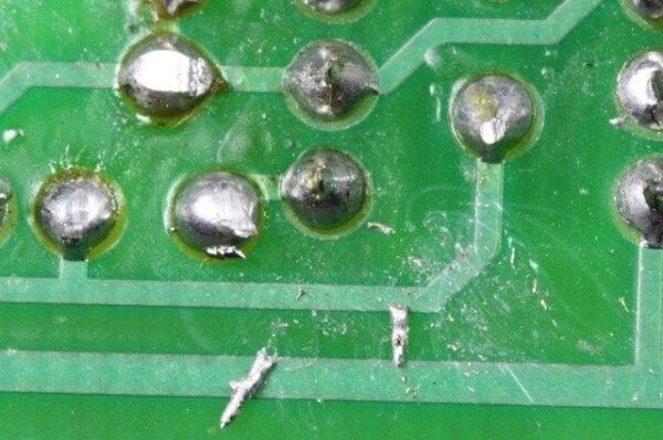
Solder Balling
Solder balling is the phenomenon of unattached solder spheres, which can create short circuits and unstable operations.
Causes:
- Humid environments affecting solder paste quality
- Aggressive or incorrect reflowsettings
- Inadequate PCB cleaning
Solutions:
- Store all materials (paste, PCBs, components) in low-humidity conditions
- Regular cleaning of PCBs during pcb fabrication and assembly
- Fine-tune reflow profiles for gradual heating
Component Misalignment/Skewed Placement
Misalignment leads to assembly imperfections such as cold solder joints, solder bridges and is more likely with miniature-sized components such as resistors, capacitors.
Causes:
- Placement machine inaccuracy or vibration on the assembly line
- Insufficient solder paste tackiness leads to movement pre-reflow
Solutions:
- Calibrate placement machines and conveyors regularly
- Choose paste with sufficient holding power
Non-Wetting/De-Wetting
If solder does not stick or recedes, the part may not connect correctly and may cause open or high-resistance joints.
Causes:
- Pad or lead oxidation
- Surface contamination (oil, dust)
- Poor flux activity or oxidation of pads/leads
Solutions:
- Store components/PCBs in dry, clean areas
- Pre-bake moisture-prone boards before paste printing
- Choose flux and solder paste matched to board metallurgy for reliable solder joints
Solder Beading
Solder beading is often observed near chip components when paste volumes are too high, encouraging short circuits.
Causes:
- Large stencil apertures causing excessive deposits
- Component movement pre-reflow
Solutions:
- Reduce paste volume for small pad areas
- Use AOI to check before committing to reflow
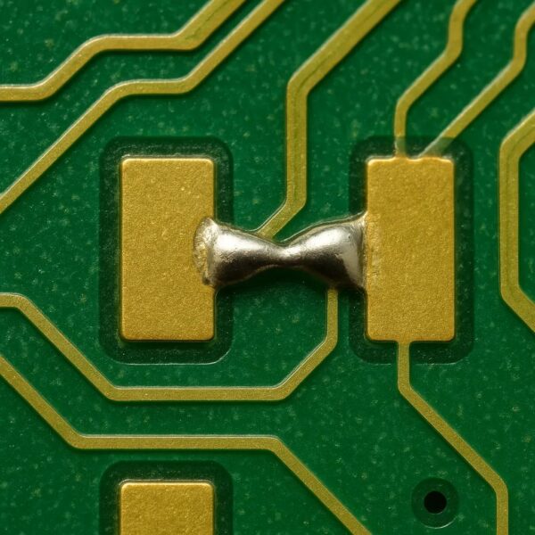
Cold Solder Joint
Cold joints are dull, weak, and susceptible to mechanical or electrical failure.
Causes:
- Low reflow temperatures or rapid, uneven cooling
- Old, oxidized solder paste
Solutions:
- Periodic profiling of ovens to ensure proper reflow temperature
- Use high quality solder paste with optimal viscosity and shelf life
- Avoid the use of expired solder paste and fluxes; store materials in climate-controlled environments
- Address uneven solderheat application on the production line by ensuring ovens have uniform temperature zones
Solder Voids / Blowholes / Pinholes
Voids, blowholes, and pinholes in solder may have a considerable effect on strength and reliability of the final assembly.
Causes:
- Outgassing from PCB fabrication residues or flux during reflow
- High paste moisture absorption or trapped gases
- Fast or incorrect reflowtemperature profiles
Solutions:
- Pre-bake PCBs to remove excess moisture before use
- Use solder paste formulations designed to minimize voids
- Slow down heating ratein the reflow oven to allow gas escape
- For high-reliability products, consider vacuum reflow equipment for void-free joints
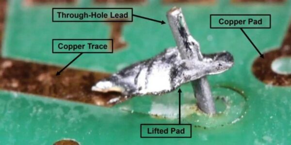
Lifted Pads / Leads / Component Damage
Elevated pads or leads and damage to components are severe assembly defects and can be difficult and expensive to correct.
Causes:
- Excessive manual rework or repeated use of a hot air rework station
- Overheating during rework, or thermal shock from rapid heating/cooling
- Mishandling of sensitive passive components like resistors or improper tool use
Solutions:
- Use gentle, ESD-safe tools and avoid aggressive soldering or repeated thermal cycling
- When reworking, use the soldering iron or hot air gently and only for the time necessary.
- Train staff on component handling and awareness of pad/lead fragility
- In the event a pad or trace is damaged, talented repair techs have the ability to reconnect them with the aid of a fine tip soldering iron and specialized adhesive tapes.
Additional Defects: Solder Paste Slump & Head-in-Pillow Effect
Solder Paste Slump
Paste slump is the phenomenon for which solder paste flows uncontrollably prior to reflow, leading to bridging and the risk of short circuits.
- Causes:High room temperature or humidity, incorrect or aging paste
- Solutions:Apply slump-retaining additive, control environment, do not wait too long between paste printing and placing
Head-in-Pillow Effect
This fault, observed in particular on BGAs, arises when the ball and paste do not fuse and leads to open circuits that can create hanging contacts.
- Causes:Warped component or PCB, poor coplanarity, incorrect reflow profile
- Solutions:Reduce board/component warpage, optimize reflow, select compatible parts
The Effect of RoHS and Lead-Free Solder on SMT Defects
The introduction of RoHS compliance and lead-free solder has altered the defect pool for typical PCB assemblies.Tin–lead vs lead-free alloys behave differently:
- The higher reflow temperatures of the lead-free solder compromise its reliability due to increasing risk of defects such as tombstoning, non-wetting, solder voids, and uneven solder joints
- Tin whiskersformation can cause latent short circuits
- Wetting performance of lead-free is less, hence the smt process is less forgiving.
How to Prevent Lead-Free Solder Defects:
- Use high-activity, lead-free compatible fluxes/pastes
- Fine-tune reflow temperature profiles for longer soak and uniform peak temperatures
- Adopt best practices for component selection and pad finishes
- Work closely with suppliers to choose the right materials for your assembly line
The Role of Inspection Tools: AOI and X-Ray in Defect Detection
Prompt and precise defect identification enables rework cost saving, yield enhancement and waste reduction. Inspection tools such as:
- SPI (Solder Paste Inspection):Checks the solder paste deposition and its volume are correct before component placement
- AOI (Automated Optical Inspection):Detects errors such as misaligned components, bridging, lack of solder, and more immediately after reflow
- X-ray inspection:Essential for hidden defects especially under BGAs/QFNs where issues such as head-in-pillow or voids cannot be observed visually
Practical Troubleshooting and Solutions Table
| Defect | Common Cause | Solution |
| Solder Bridging | Excess paste, stencil design | Clean/optimize stencil, SPI, rework |
| Cold Joint | Low temp, poor wetting | Reflow with iron/hot air, new paste |
| Tombstoning | Uneven heating/paste | Pad/footprint review, reflow profile |
| Voids | Outgassing, moisture | Pre-bake, slow heating, vacuum reflow |
| Open Circuit | Insufficient paste, oxidation | Squeegee, fresh paste, surface prep |
| Short Circuit | Bridging, balling, beading | Stencil/paste optimization, AOI, rework |
| Misalignment | Placement error, PCB warp | Machine calibration, paste chemistry |
| Lifted Pads | Overheating, rough handling | Rework station control, ESD training |
Process Optimization: Preventing SMT Assembly Defects
The following are practical measures to avoid SMT assembly defects, and to increase yield and quality:
Optimize Stencil and Solder Paste Application:
- Use precise aperture sizes for every component
- Clean stencil frequently and review paste condition
- Calibrate squeegee pressure and speed
Component Handling and Selection:
- Vet suppliers and choose the right components for SMT assembly
- Ensure compatibility with the SMT process; watch for maximum temperature and moisture sensitivity levels
Reflow Profile Tuning:
- Develop and monitor profiles specific to each assembly/circuit
- Avoid running incorrect temperature profiles, which may lead to cold joints and burn defects
Regular Inspection and Data Collection:
- Leverage inspection tools for all critical process points
- Record defect trends to spot patterns, enabling preemptive fixes
Continuous Training and Partnering With a High-Quality Manufacturer:
- Update staff on rework and inspection best practices
- Consider the benefits of partnering with a high-end contract manufacturer such as LingKey, which offers DFM support, the ability to detect advanced defects, and ability to streamline processes for a stable and high-yield SMT assembly production.
Conclusion: Building a Reliable SMT Assembly Process
As described in this guide, knowledge of the defects arising in the SMT process—from solder bridging to head-in-pillow –is essential for all assembly lines. By following the above solutions and optimizing each step (or partner/tool, if you need them), you’ll have a massive impact on your rework costs and overall yield.
A perfect quality PCB starts with your design and goes through every process of assembly and ends with reliable inspection equipment. Learn these rules for a successful SMT assembly and world class electronic products.
Also, working with a professional pcb assembly manufacturer is essential for consistent quality and less defect. LingKey provides you with high-level of SMT assembly services with rigorous process control, total inspection systems and strong engineering support to assist you in increasing yield, minimizing rework and to supply dependable electronic product.


