PCB Overmolding: Injection Mold Guide
Introduction to PCB Overmolding
Modern electronics require dependable performance, even in the harshest conditions. It’s this demand for reliability that has led PCB overmolding to become a niche yet critical manufacturing process for printed circuit board assemblies (PCBAs). Overmolding shields the PCB and its electronic parts with an unparalleled level of protection, mechanical strength, and performance. In this post, we will cover the entire process in detail of pcb overmolding, the typical overmolding process step, and how overmolding can keep your technology working flawlessly, regardless of where it goes.
What is PCB Overmolding?
The PCB overmolding is the use of injection molding method to cover a circuit board and its sensitive components with a strong, customized shell. In other words, overmolding circuit boards is the process of inserting the PCB—or the PCBA—into a mold cavity, and then injecting an overmolding material into the mold. This makes for a smooth, protective coat around the PCB.
Overmolding is not just a matter of protection – it revolutionizes the way PCBs are packaged and enables assemblies to be more compact and the use of bulky, traditional enclosures is eliminated. The result is a highly efficient process that makes it possible for electronic components to function reliably—even in the presence of heat, moisture, chemicals and severe mechanical impact.
Overmolding makes use of injection molding machines which are specially modified to suit the low and high pressure thermoplastic methods. The PCB is usually held in a fixture, which enables the encapsulant material to flow uniformly around the PCB and fully cover it.
Why Overmold a PCB? Key Benefits & Advantages
The benefits of overmolding PCBs are extensive, driving its adoption across industries:
- Impact Resistance & Mechanical Durability:The shield makes the impact of the electronic assemblies stronger and absorbs shocks and vibrations that would break fragile parts.
- Environmental Protection:Overmolded circuit boards are waterproof, dustproof and sealed against oil and chemicals, the best way to get IP67/IP68 ratings.
- High Temperatures Endurance:Specialized overmolding materials for PCB with high thermal stability are used to shield delicate elements of a PCB from overheat and thermal cycling.
- Aesthetic Flexibility:Overmolding allows for integrated colors, logos and even QR codes, which are molded into the device surface.
- Simplified Assembly:Overmolding can also mean less parts—doing away with screws, seals, and traditional hard-shell cases. Overmolding Pcb lead to the simpler and less mistake assembly process.
- Electrical Insulation:A seamless overmolded shell guards from arc-over, rust and moisture that can cause board failures.
The advantages of PCB overmolding are what make it the technology of choice in automotive, consumer electronics, medical, and industrial applications.
PCB Overmolding Techniques & Injection Molding Process
Main Overmolding Process
The process of PCB overmolding typically includes the following steps:
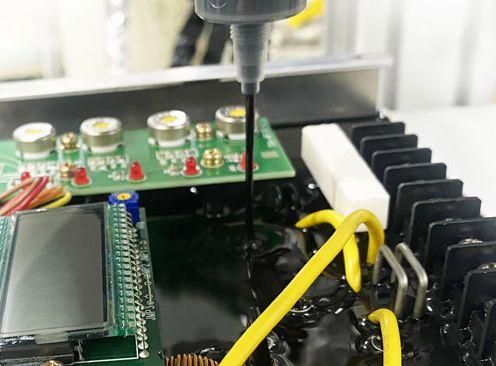
- Preparing the PCB:Pre-testing, cleaning and drying are necessary. Some assemblies employ a soft gel prior to the primary overmolding to insulate fragile components.
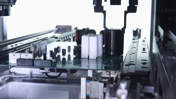
- Molding Machine Setup:A low or high pressure injection molding machine is equipped with custom fixtures. Fixturing holds the PCB in place and directs the flow of material to provide uniform encasement.
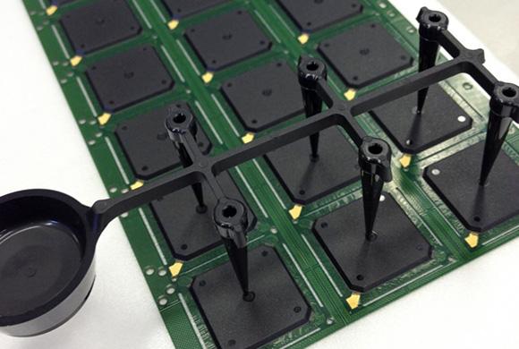
- Placing and Sealing the PCB:The PCB along with all the electronic components are placed in the mold. It is held to the exact distance by support structures or spacers for a uniform flow of the overmolding material around the PCB.
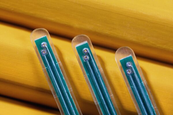
- Injecting the Overmolding Material:With injection molding, the selected resin (for example, TPU, TPE, PA, PC or silicon) is heated to a lower melting temperature if for sensitive assemblies, and then injected quickly to surround the PCB.
- Cooling and Demolding:After cooling, the müti-part shell becomes solid around the PCB. Controlled cooling is essential to prevent warpage and ensure good bonding.
- Post-Molding Inspection and Testing:Visual and electrical examinations as well as environmental exposures verify the absence of defects, including bubbles, delaminations, or cracks.
This process ensures that the overmold provides structural and environmental protection to sensitive electronics.
In modern manufacturing environments, precision tooling, material flow control and thermal management are tightly integrated, allowing a company like LingKey to deliver consistent encapsulation and eliminate process related defects (voids, delamination, or stress damage) in the overmolding process.
Common Materials Used in PCB Overmolding
| Overmolding Material | Typical Use Cases | Notable Features |
| TPU (Thermoplastic Polyurethane) | Wearables, consumer electronics | Flexibility, abrasion resistance |
| TPE (Thermoplastic Elastomer) | Automotive, connectors, rugged devices | Excellent shock absorption |
| PA (Polyamide/Nylon) | Industrial, under-hood automotive | High strength, chemical resistance |
| PC (Polycarbonate) | Lighting, sensors, enclosures | Optical clarity, UV resistance |
| Silicone (Liquid Silicone Rubber) | Medical devices, waterproof modules | Hypoallergenic, wide temp range |
| PPS (Polyphenylene Sulfide) | High-temperature, harsh environments | Heat & chemical resistance |
PCB overmolding materials are selected for their mechanical, thermal and chemical characteristics. During molding, material flow is closely monitored to ensure precise coverage of the sensitive components of the PCB without stressing them.
PCB Overmolding Process: Preparation to Post-Processing
Let’s explain each stage of the circuit board overmolding process with injection molding:
Preparing the PCB: PCB components and electronic components are washed, inspected and dried. For delicate kits, a soft elastomeric gel can be applied prior to the main overmolding to protect delicate parts.
Insert/Fixture Placement: The PCB assemblies are clamped into a nest in the mold cavity to prevent the board from moving and to allow the overmolding material to flow consistently about the PCB.
Overmolding Material Selection and Injection: Based on the requirements of the device, the engineer chooses from the standard materials available for PCB overmolding—typically they lean towards ones that are lower melting temperatures so that the heat doesn’t damage sensitive components. The injection molding machine injects the resin into the mold, covering the PCB and closing all the gaps.
Material Flow and Solidification: Regulated flow of material results in no bubble formation and full and uniform coverage. The cooling then follows quickly and solidifies the protective film.
Post-Molding Inspection: Every overmolded PCB is subjected to visual and electrical testing. Environmental testing (to IP67/IP68, and higher for certain applications) guarantees that the assembly and its delicate components are sealed.
Best Practices and Design Considerations for Overmolded PCBs
To get the most benefits of PCB overmolding, engineers must work together early in the process and consider:
- Board layout edge clearance:Keep the distances from the edge to the critical parts so the protective layer fully covers the PCB without straining the components.
- Keep-out zones and gate placement:Design keep-outs and an injection port location to prevent resin from flowing over sensitive areas such as exposed connectors or LEDs.
- Material compatibility:Select the appropriate CFR for the PCB overmolding materials to suit your temperature and chemical exposure requirements, particularly for high temperatures or corrosive environments.
- Temperature and Pressure Control:Use low melting or low pressure resins to shield sensitive components from thermal and mechanical stress during molding.
- Fixture Precision:The precision of the fixture is important to prevent the board from shifting and for an even distribution of overmolding
Quality Control & Preventing Defects in PCB Overmolding
Typical defects are bubbles, delamination and cracks which appear as a result of poor material flow or too little drying.Rigorous quality control includes:
- Detailed visual inspections for surface and flow defects.
- Electrical tests to verify circuit continuity and no shorts or signal loss.
- Environmental tests to simulate the harsh operating environments (humidity, temperature cycling, mechanical shock, vibration) are conducted to verify that the protective layer results in complete environmental enclosure.
- The adhesion tests are conducted to verify that the overmold material remains tightly bonded to the PCB enabling it to shield the electronics during the life of the product.
PCB preparation, injection molding process control, and post-mold inspection must all be performed to ensure overmolded PCBs will perform and are as reliable. The result of these rules is a much lower risk of defects such as cracking, bubbles, delamination or insufficiency of coverage.
Applications of PCB Overmolding Across Industries
PCB overmolding now is a norm in industries where protection and reliability of electronic component are a must, particularly in high temperature, harsh chemical or physical abuse environment.
Automotive: Overmolding makes sensitive components of the PCB such as sensors, ECU modules and under-hood control units resistant to vibration, oil, chemicals and extreme heat. For instance, heat-sensitive automotive sensors can be shielded from damage through low-pressure molding and material flow control.
Medical Devices: In wearable monitors and implantable electronics, overmolding provides a biocompatible, waterproof, and cleanable surface. Prior to the main overmolding process step, silicone overmolding is frequently combined with gel layers for additional protection of sensitive electronics.
Consumer Electronics: Overmolded PCBs can be found in smartwatches, earbuds, remote controls, and game controllers, as the added impact protection and dustproofing, along with custom branding (colors, logos, textures), provide value and extend product life.
Industrial Controls & IoT: Overmolded circuit boards in rugged PLC units, outdoor sensor hubs and weather stations provide the reliability required for remote and extreme environments. The encapsulated package withstands UV, chemical and water.
LED Lighting: Outdoor and underwater LEDs drivers are able to take advantage of the environmental sealing with pcb overmolding and a layer of protection from heat, moisture, and vibrations, resulting in a longer life of operation for the LEDs.
Overmolding vs. Potting, Encapsulation, and Traditional Enclosures
Selecting between overmolding, potting or conventional enclosures is a matter of what the environment the product will be exposed to, and the level of ruggedization required.
| Property/Method | PCB Overmolding | Potting/Encapsulation | Traditional Enclosure |
| Environmental Sealing | Excellent (IP67/68+) | Good (resin-dependent) | Moderate (gasket-reliant) |
| Impact Resistance | High | Moderate | Variable |
| Aesthetics/Branding | High | Low | High |
| Assembly Complexity | Low | Moderate | High |
| Serviceability | Low | Low | High |
Overmolding is an advanced manufacturing process that combines the benefits of environmental and mechanical protection with the ability of creative product design and branding – all accomplished in one efficient process.
Choosing a Professional PCB Overmolding Partner
Finding a seasoned manufacturer is essential, as overmolding is a complex process that requires extensive knowledge, specialized machinery, and rigid process control. LingKey offers a professional pcb overmolding solution with excellent engineering support, advanced injection molding technology and total-process quality control to protect sensitive electronic assemblies reliably.
- Demonstrated experience with overmolding circuit boards in your industry.
- Skilled engineers who understand both PCB packaging and injection molding.
- Full spectrum of support, from DFM review to moldmaking and post-process testing.
- Access to a broad selection of popular materials used in PCB overmolding to find the perfect fit for your project.
Before you commit, ask about their molding machine capabilities, process for material selection and quality assurance, and examples of past projects.
Cost, ROI, and Economic Benefits
Although the initial cost associated with tooling a plastic overmolded PCB can be more than basic potting or opting to not use a protective layer, the benefits of PCB overmolding recoup that outlay:
- Lower assembly costsdue to reduced part count and assembly time.
- Longer life for the products and reduced warranty The overmolding allows critical electronics to withstand impact, moisture and chemical contact.
- Integrated branding means no labels are used, and a reduction in the number of join lines means fewer places for water or dust to get inside.
Future Trends in PCB Overmolding
- Sustainable and recyclable thermoplastics are becoming more popular as demands for sustainability increase.
- Novel engineering solutions merge gel application prior to the primary overmolding process for additional cushioning in ultra-fine assembly.
- Intelligent control of molding machines, simulation-based design, and in-line inspection systems are now pushing the boundaries of quality and consistency further and further.
- Overmolding ensures the consistent production of ever-smaller, more reliable and more branded electronics for every industry.
Frequently Asked Questions About PCB Overmolding
Can any PCB be overmolded? Most rigid and rigid-flex PCBs are well suited. Flexible boards, or fragile boards in general, might require special jigs and/or lower melting point resins so that they won’t be damaged.
What about high temperatures? In case the device needs to be used exposed to high temperatures, select the materials for PCB overmolding with broad thermal windows and good thermal stability, for example PA or PC.
What are the main overmolding process precautions for delicate components? Use soft cushioning gel or choose low pressure/low temperature materials. Sophisticated process control guarantees that fragile solder joints and chips are not damaged.
Are overmolded PCBs repairable? Generally no. They are built for maximum reliability, and are usually replaced if they become damaged.
Does overmolding add weight or bulk to my device? Small amount, as the protective jacket is custom designed with a thickness sufficient to just wrap around the pcb and provide maximum protection.
Conclusion: Is PCB Overmolding Right for Your Product?
As electronic device durability evolves, PCB overmolding is the best solution for engineers looking for maximum reliability, efficiency and aesthetics. Overmolding fully encases your printed circuit board assemblies in a customized protective layer, protecting sensitive parts from the outside environment and streamlines your manufacturing. When paired with the right partner, materials, and design strategy, overmolding can provide you with the next generation solution for extreme environments and future-ready electronics.
If your product needs long life, strong environmental protection, co design or easy assembly, try to take consideration on the benefits of pcb overmolding for your next product launch. Talk to an expert now on the potential impact of overmolding circuit boards with injection molding on your electronic products.
Also, the pcb overmolding benefits cannot be fully realize without the support of experienced manufacturer. LingKey provides a full spectrum of services, including design optimization, material selection, precision molding and testing to enable customers to achieve high reliability, lower assembly complexity and uniform product performance in challenging environments.


