Hard Gold PCB Finish & Thickness
Introduction
Hard gold PCB processing is of great importance in today’s electronics, especially for the main applications such as high-reliability connector and contact point. In pcb assembly, the type of PCB surface finish affects not only the manufacturability but also the long term electrical and mechanical reliability. Gold has unique benefits such as being highly corrosion resistant, having a low contact resistance and enabling signal integrity in high frequency applications. This definitive guide to hard gold pcb discusses its advantages and applications, describes the process steps in the hard gold pcb manufacturing process, and also provides a comparison of gold finishes to assist in selecting the appropriate finish for your pcb fabrication and assembly.
Key Takeaways
- Hardened gold offers the best wear and corrosion resistance in pervasive contact areas.
- The gold over nickel stack, with a nickel underlayer serving as a barrier, offers the best in electrical and mechanical properties.
- Hard gold can survive many, many connection cycles and is the finish of choice for applications which have high reliability.
- In pcb layout and pcb assembly, selectively plating only high-wear areas can reduce cost.
- Hard gold plating standards and thickness requirements must be followed to ensure plating quality and
- ENIG vs hard gold: Both utilize gold and nickel, but are distinct in performance in the abrasively-stressed regions.
What is Hard Gold PCB?
Definition and Distinction
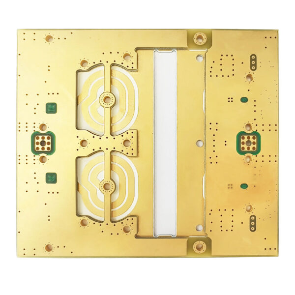
A hard gold PCB is a circuit board on which a layer of hard (alloyed) gold has been plated on the top of nickel in selected areas, typically on PCB edge connectors (gold fingers) and high cycle points of contact. This gold over nickel structure is designed to produce a PCB surface that is mechanically wear resistant and can be subjected to repeated insertions, where gold offers low contact resistance and the underlying nickel barrier layer provides durability by functioning as a barrier between gold and the underlying copper. The plating time, as well as the current density during plating, influences the total thickness of gold and nickel.
Hard Gold PCB vs Hard Gold Plating for PCBs
Similarly to the finished board, the hard gold plating for pcb is also defined as electroplating. This method applies gold (alloyed for hardness) selectively onto contact points or gold finger pads so only the areas that actually need the properties of hard gold receive this premium finish.
Comparison to Other PCB Finishes
Is ENIG better than hard gold is a frequently asked question. Both finishes incorporate gold and nickel, however the formulation and application processing vary. Hard gold is electroplated and has a thicker layer of gold, providing mechanical strength in the areas of wear, while ENIG is chemically deposited, you get a thin layer of pure gold that is the best for solderability. Soft gold is pure gold (not alloyed), used for wire bonding, not on wear surfaces.
Key Properties of Hard Gold Plating
In constructing PCBs and during assembly, Excellent material properties of Hard Gold mainly dictate its application:
- Thickness of hard gold plating:Varying from 1 to 100 micro inches, with final results being application based in the terms related to the thickness standards (normal golden finger necessities: 30-50 microinches).
- Nickel underlayer thickness:Typically, 100–200 microinches; nickel serves as a barrier to stop the diffusion of copper and also acts as the mechanical support for the gold.
- Gold and nickel combination:This stacking result in the wear resistance and corrosion protection better than that of copper and gold
- Electrical conductivity:Gold offers minimum contact resistance which results in high signal integrity in critical application such as those found in the aerospace or data communications industries.
- Mechanical hardness:Hard gold is significantly tougher than soft gold or ENIG under wear
- Finish compatibility:Hard gold finishes are compatible with most pcb assembly methods, but are particularly popular for pcb edge and high-use connectors.
Understanding Hard Gold Plating Thickness for Optimal Performance
The performance of gold plated PCBs is impacted by the thickness of hard gold plating.Use these tips for best results:
- A thin layer of gold (~1-5 μin) is enough for static test pads with low wear, but most applications such as finger and connector plating require more plating (30–50 μin).
- Gold plating (up to 2.5μm) can be specified for extreme wear and mission critical
- Nickel thickness:Be sure to monitor these also to have a solid film before the gold is plated. A lack of nickel can affect the durability, since the nickel undercoat serves as a barrier.
- The plating time and current density during electrodeposition play a major role on quality and uniformity of the plated film, and consequently, thickness and adhesion.
Hard Gold PCB Manufacturing Process Steps
1. PCB Fabrication and Surface Preparation
Quality starts in the pcb fabrication process: The copper is etched to define the traces, gold finger pads and contact areas, and then cleaned to remove oxides and contaminants from the surface of the PCB.
2. Nickel Plating (Acts as a Barrier)
A layer of nickel (~100–200 microinches) is electroplated over the copper. This nickel underlayer serves as a diffusion barrier and enables the mechanical stability of the hard gold.
3. Gold Electroplating (Hard Gold Areas)
Then the electroplating process plates gold, alloyed with either cobalt or nickel for hardness, to the specified pads and edge connectors. This gold is less than 99.9% pure gold making it more durable than the soft gold. In projects where designers require hard gold, the plating quality controls are tight.
4. Soldermask and Silkscreen Application
These steps protect non-contact areas and provide labeling.
5. Quality Testing and Inspection
Hard goldThickness and adhesion of thick gold plating are tested by X-ray fluorescence (XRF), tape testing, and microscopic evaluation testing. Critical use boards can also be subjected to functional and environmental testing for performance verification.
Table: Typical Process Stack-Up
| Layer | Material | Typical Thickness | Key Role |
| Copper Traces | Copper | 35–70 microinches | Conductive paths |
| Barrier Layer | Nickel | 100–200 microinches | Diffusion/Mechanical barrier |
| Gold Plating (Hard) | Gold Alloy | 30–50 microinches | Low resistance contact surface |
| Soldermask (Optional) | Polymer | – | Mechanical/Electrical isolation |
Hard Gold Plating Standards: Ensuring Quality and Compliance
The requirements for the thickness of hard gold plating are dictated by industry standards and test methods such as IPC-6012 and MIL-STD-275Key specs include:
- Gold thickness and uniformityat all plated locations.
- Minimum nickel thicknessto prevent copper migration.
- Adhesion and porosity checksto assure plating quality.
- In aerospace or other critical application, the manufacturer can provide a certificate that the item meets all the required standards.
Key Applications of Hard Gold Plating in PCB Design
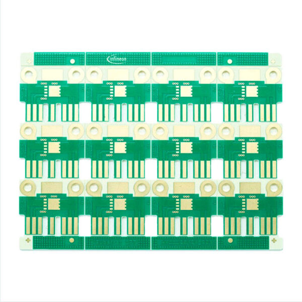
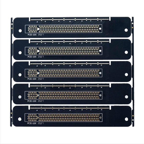
- PCB edge connectors and gold fingers:Almost every memory module, expansion card, or high-reliability PCB plug-in board is plated with hard gold over nickel for its edge fingers. These are the main applications that require high durability with excellent electrical performance. Gold has a low contact resistance and provides a uniform and stable connection that is essential for communications at high speed and for multiple connect/disconnect.
- Contact points and high-use connector pads:Every point on a PCB that is anticipated to come into contact with hardware repeatedly, like test pads, card-edge connectors, or power modules, will benefit from the enhanced wear and corrosion resistance offered by hard gold. As an illustration, in the PCB assembly lines where test points undergo recurrent probing, a hard gold plating prolongates the board life to great extent.
- Switch contacts and industrial controls:In industry applications, gold plating offers a suitable level of stability and durability for exposure to chemicals and physical contact. Hard gold is resistant to extreme environments, and is widely used on your PCB in these critical applications.
- Applications requiring high reliability:Industries such as aerospace, defense, and automotive electronics have very stringent requirements for interconnect robustness and signal integrity. In this case, thicker gold layers (up to 100 microinches) may be specified in order to ensure reliability for a number of thousand cycles and in harsh environments.
Benefits of Hard Gold PCB
In comparison with other platings, hard gold offers a range of key benefits that make it the best choice for applications that require the highest level of performance:
Unrivaled wear resistance and toughness Hard gold is suitable for application in areas of frequent predictable physical contact e.g. gold finger connectors or edge pads.
Stable, low contact resistance The gold over nickel—also known as the “nickel underlayer and gold stack” combination provides a low, stable resistance that is essential for signal integrity in the high frequency application. This characteristic is critical in particular for memory busses, data channels and RF interconnects.
Excellent Corrosion Resistance Gold is highly resistant to oxidation and chemical attack, so it retains its electrical performance for long periods of time which makes it necessary in applications such as in the field of aerospace, medical and industrial controls.
High-speed signal compatibility Because of its chemical stability and smooth surface, hard gold distorts signals and causes crosstalk the least, and this is the main reason we use it when working on digital systems running at the gigahertz range.
Long-term cost savings Although hard gold is more expensive to plate, this is more than offset by longer life, fewer failures and replacements -particularly for plug-in modules and hi-reliability products.
Limitations of Hard Gold PCB
Despite its strengths, hard gold is not perfect for every scenario:
Higher cost per unit area Because of the value of the gold and the precision needed to plate, this finish is normally applied only to the edge connectors and dedicated contact pads, not to the entire surface of the PCB.
Solderability and assembly issues Very high gold thickness (over 50 microinches for wirebonding) will produce problems such as gold embrittlement in solder joints. For the majority of SMT pads, ENIG is the preferred finish unless long life under contact is required.
Bonding limits Soft gold is a pure gold and has a very good application for wire bonding because it is soft and easily deforms. The hardness of hard gold (due to the addition of alloying elements such as nickel or cobalt) makes it suitable for contacts, but it is not the best for fine wire bonding in chip pads.
Impact on the environment If plating processes are not managed for sustainability, they can produce poisonous waste from solutions of copper, nickel and gold.
Factors to Consider Before Using Hard Gold
Before you request a hard gold finish on your board, consider the following design and fabrication points:
Type of application and layer thickness Wear only require use of hard gold for areas with high physical contact or where sliding/plug-in movement occurs.
PCB layout and fabrication guidelines Ensure that all hard gold areas are well defined in your gerber files along with your fabrication notes. Just solder all the gold finger pads that you should connect for the high-cycle use and leave the rest as ENIG or HASL to save money.
Stacking and underlayer quality Make sure the thickness and uniformity of the nickel underlayer is appropriate-this is non-negotiable, since any gaps in the nickel coverage will result in early failures.
Plating quality control Impose strict monitoring of the thickness of hard gold plating,taking into account thickness standrads in relation with end application. Request XRF or equivalent documentation with your delivery.
Hard Gold vs. Other PCB Finishes
ENIG vs Hard Gold
Solid gold and ENIG finishes both utilize gold and nickel layers, but have their own advantages:
- ENIGconsists of a very thin layer of gold chemically plated over nickel(typically just 1-5 microinches), which provides excellent solderability for surface mount devices but is not good wear resistant.
- Hard gold is processed by electroplating to have a thicker plating layer and better wear properties, thus it is suitable for applications in gold finger contacts and other high-use areas.
Table: ENIG vs Hard Gold
| Feature | ENIG (Electroless) | Hard Gold (Electroplated) |
| Gold Thickness | 1–5 microinches | 30–100 microinches |
| Wear Resistance | Low | Very High |
| Solderability | Excellent | Good at lower thickness |
| Use Case | SMT/BGA pads | Edge connectors, contacts |
| Plating Process | Chemical | Electroplating |
Soft Gold vs Hard Gold
Soft gold is solid gold (99.99%) and is not alloyed, it is mainly used for wire bonding; hard gold is alloyed (with cobalt/nickel) and electroplated for wear resistance, it is also less bondable and better for wear.
Best Practices for Hard Gold Plating in PCB Design
Confine hard gold to the essential areas Limit application to the edge connectors, contact pads or switch areas that need to be robust.
Thickness Specification for a gold and a nickel layer Always specify the needed gold and nickel thickness for each location of hard gold in the drawing.
Make sure that all the hard gold regions are tied together For uniform plating, all the gold finger and pad areas must be electrically connected in pcb layout while plating.
Plating time and current density should be monitored The electroplating process needs to accurately control these parameters to satisfy the requirements of hard gold plating and to provide consistent and dependable coverage.
Hard Gold Plating Troubleshooting: Common Issues and Solutions
Poor current density and/or pot positioning during plating may cause inadequate or uneven plating etc. Always inspect the process and request for the verification report.
Nickel underlayer exposure Damage or overuse can expose nickel, raising cr and this risk is eliminated with proper qc and use of thicker gold.
Cracking or delamination is frequently an indication of inadequate pcb surface preparation or too much internal stress. Make sure your supplier adheres to best practices for both pcb fabrication and plating.
How to Choose the Right Hard Gold PCB Manufacturer
When your product’s reliability depends on gold plating, always:
- Select a supplier that has pcb assembly experience, be it in critical applications like medical, automotive, or aerospace.
- Request documentation for all thicknesses of gold and nickel plating and quality tests (XRF results, adhesion tests).
- Make sure the manufacturer knows the finish for your pcb and can adapt the process to your particular pcb layout.
- Ensure the supplier complies with all industry and environmental requirements.
At Lingkey, we have the powerful solution to precision hard gold plating with strict quality control and compliances of the industry to make sure the plating thickness, adhesion and reliability are consistent for high end PCB, which is indicative of our high performance PCB Application.
Frequently Asked Questions (FAQs)
What is the typical thickness of hard gold on a PCB?
- Gold:30–50 microinches for edge connectors, up to 100 for extreme cases.
- Nickel:100-200 microinches, it is always applied first serves as the primary mechanical barrier.
Is hard gold PCB solderable?
- Yes,up to a moderate thickness. For SMT assembly, ENIG or OSP is recommended for improved solder joint reliability, however, hard gold should be specified for mechanical wear applications.
Can hard gold and ENIG/soft gold be used on one board?
- A lot of designs combine finishes: hard gold contact points with ENIG for the SMT pads, giving the best of both cost and performance.
How does gold plating affect signal quality at high frequencies?
- The stack up of gold and nickel ensures the best signal integrity and high frequency performance with clean transitions and low insertion and return losses.
How do manufacturers ensure plating quality?
- By means of detailed control of plating bath chemistry, plating time and current density and by regular testing with XRF or tape adhesion k test according to international standards.
Conclusion: Mastering Hard Gold Plating for PCB Success
In high-reliability high performance electronics, particularly when connectors or test points undergo repeated cycling or have become subject to harsh environments, hard gold PCB finish is the gold standard. Utilizing the gold over nickel synergy -where nickel is the barrier layer -you get low resistance, corrosion resistance and excellent mechanical robustness. The right hard gold plating rate, accurate thickness control and cautiously processing, make the PCB surface really shine for strong long-life performance.
Always do business with suppliers that are professional and knowledgeable, insist on industry-standard compliance, and apply the knowledge from this guide to know your finishes forwards and backwards for your next mission-critical application. If you’re designing the next great space craft, airliner, industrial controller-hard gold is the edge your project deserves.
Lingkey is dedicated to providing high-reliability hard gold pcb solutions with precise plating control and stable manufacturing process to make your products perform stable under high end everments.


")
