Understanding USB Pinout: From Theory to Practical PCB Design
Universal Serial Bus technology forms the basis of present-day connectivity and data transfer. As you charge electronic items, provide for rapid data exchange between products, or design advanced USB PCBs for high-performance applications, complete USB pinout comprehension is integral for performance and reliability. In our USB guide, we will cover everything—types of USB connectors, signal integrity, pin arrangements, industry best practice for PCBs, and debugging—to give you high-quality, professional USB PCB design outputs.
What is a USB Pinout and Why Does It Matter?
A USB pinout defines every specific function assignment and setup for each electric contact (or pin) within a USB port or connector. There is a designated function assigned for every pin, including supplying a stable power source, high-speed data signal transfer, as well as ground integrity. Pinout mapping is the key location in USB circuits, where it forms the foundation for stable connectivity, rugged device communication, and USB standard compliance.
If you design or maintain any electronic device that uses USB, understanding pinout configuration is required for:
- Safe and efficient power delivery (including USB Power Delivery, or USB-PD)
- Reliable data transmission and high speed USB signal transfer
- Preventing USB connection issues, device failures, or even damage
- Achieving peak signal integrity and minimization of EMI when transferring data between host and device
Every USB PCB, whether for hosts, peripherals or chargers requires careful matching between cable pinout and physical stackup on your board, along with spacing requirements and trace width considerations for data and power lines.
Brief History & Evolution of USB Standards
USB standards have advanced rapidly since their introduction to address users’ increasing demand for high-quality, high speed USB solutions.
| USB Version | Release Year | Connector Types | Max Data Rate | Power Delivery (PD) |
| USB 1.0 | 1996 | Type-A, Type-B | 12 Mbps | 2.5W (5V, 0.5A) |
| USB 2.0 | 2000 | Type-A, Type-B, Mini | 480 Mbps | 2.5W |
| USB 3.x | 2008-2017 | Type-A, Type-B, Micro-B, Type-C | 5–20 Gbps | Up to 100W (with Type-C) |
| USB4 | 2019 | Type-C | Up to 40 Gbps | 100W (USB-PD) |
Type-A and Type-B were widely adopted for years, but USB-C cables now set new standards in reversible design, transfer speed, and power capabilities.
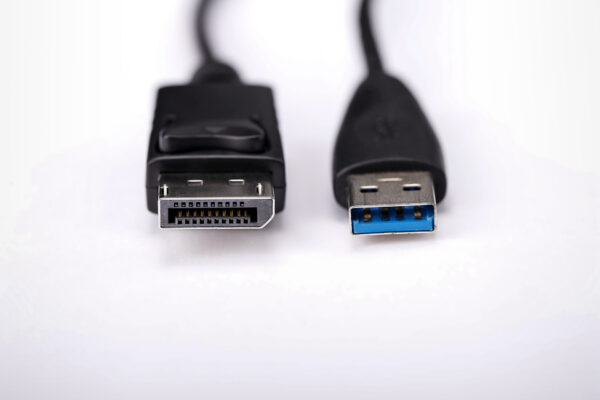
USB Connector Types and Their Applications
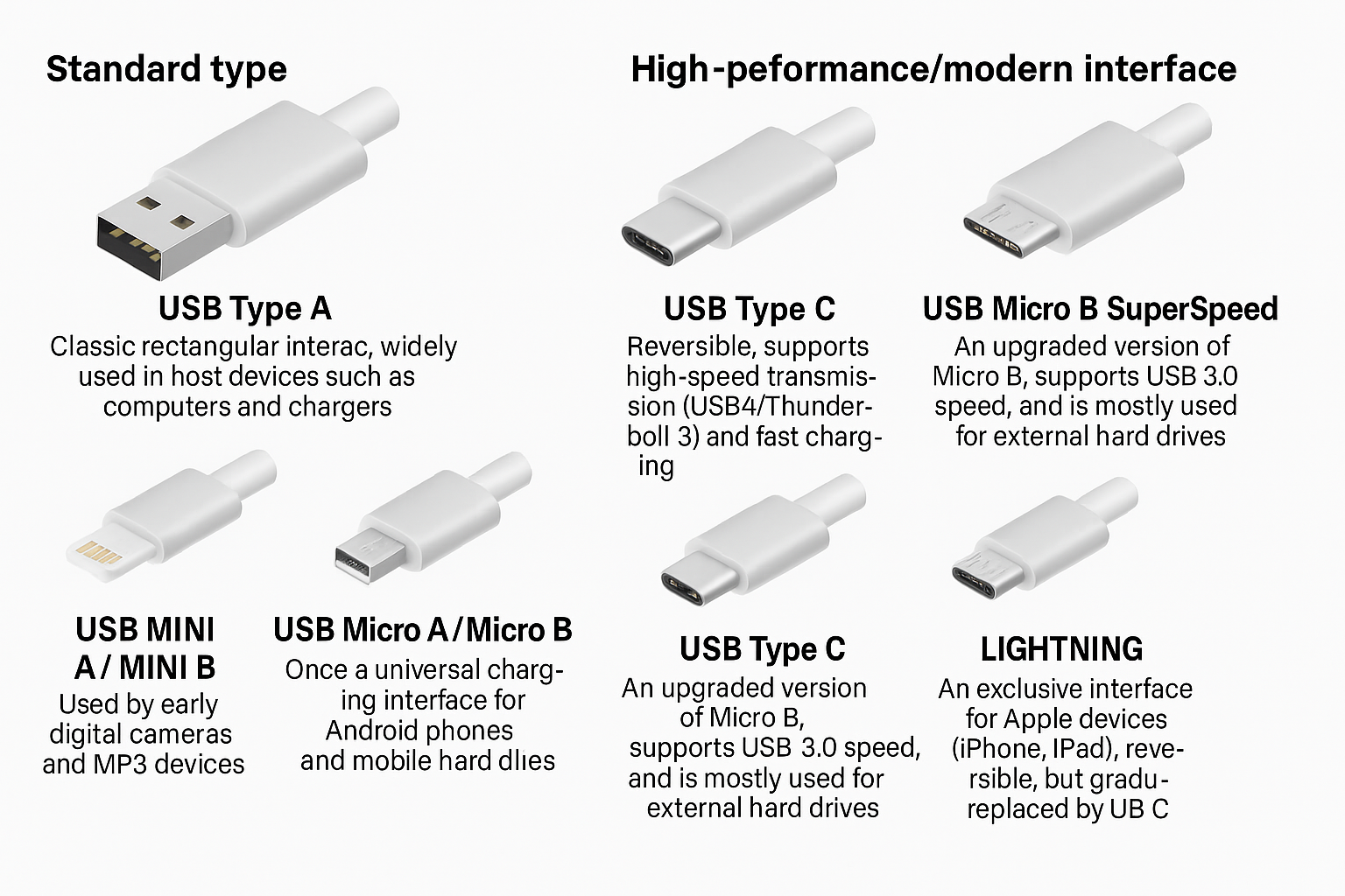
The choice of USB connector directly influences pinout, cable and connector choices, device orientation, and maximum data or power capacity.
USB Type-A: Classic rectangle, commonly used in host devices (PCs, TVs). Four basic pins for VBUS, Ground, D-, D+, and expanded pins for SuperSpeed in USB 3.x. Applications: Computer peripherals, storage drives.
USB Type-B: Squarer-shaped, mostly used for devices like printers and scanners. Applications: External hard drives, printers.
Mini-USB and Micro-USB: Smaller form-factors for portable devices. Micro-USB, with its ID pin, supports OTG (On-The-Go) for dynamic host and device switching, but has largely been replaced by USB Type-C.
USB Type-C: Reversible, compact, and powerful. Supports up to 24 pins (including CC1 and CC2 for orientation and negotiation), SuperSpeed data pairs, SBU for sideband use, supports USB-PD for up to 100W PD, and enables alternate modes. Applications: Modern smartphones, laptops, docking stations, and more.
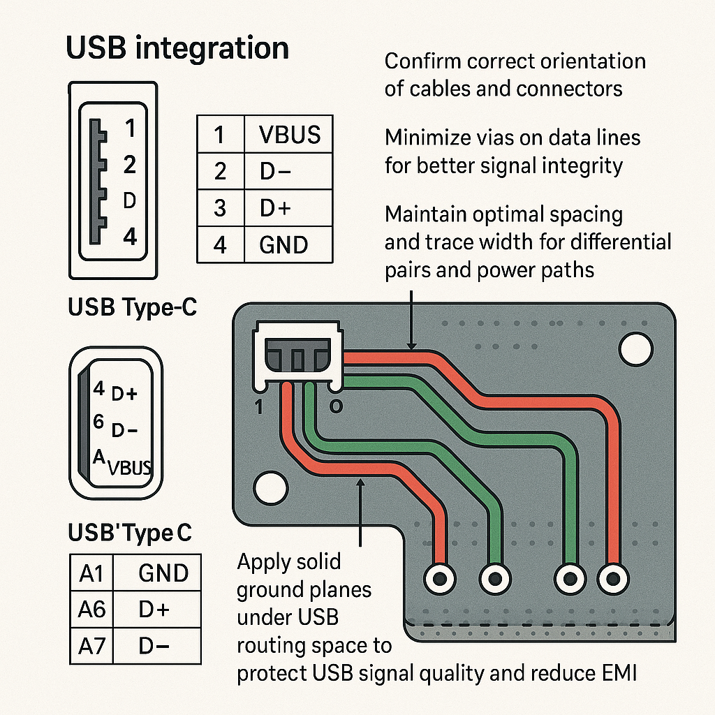
Detailed USB Pin Configurations (Pinout) by Connector
A correct USB pinout allows for high-quality, high speed USB circuits. Here’s a summary table emphasizing the most important pins for each connector:
| Pin # | Type-A | Type-B | Mini/Micro | Type-C (partial) |
| 1 | VBUS | VBUS | VBUS | A1/B12 VBUS |
| 2 | D- | D- | D- | A2/B11 D- |
| 3 | D+ | D+ | D+ | A3/B10 D+ |
| 4 | GND | GND | ID | A4/B9 VBUS |
| 5 | GND | GND | GND | A5/B8 CC1, SBU1 |
| 6-9 | (SS pairs) | (SS pairs) | — | SuperSpeed, SBU |
| 10-16 | — | — | — | CC2, SBU2, Sideband |
USB-C pinout is unique for containing both CC1 and CC2 for orientation detection, and multiple SuperSpeed pairs to ensure high-speed, bidirectional data transmission and performance and reliability under any device orientation.
USB Pin Functions: Power, Data, Ground, and More
- VBUS (Power Pin):Provides the stable power supply to the device. Designers must consider trace width and stackup to prevent voltage drop and overheating for high current USB PD applications.
- GND (Ground Pin):A continuous reference required for isolation, shielding, and error-free USB signal operation.
- D+ & D- (Data Pins):Differential signal pair responsible for all USB data transfer, including isochronous, bulk, control, and interrupt transfer modes. Differential routing with tightly matched spacing ensures proper data transmission and minimizes crosstalk between adjacent traces.
- SuperSpeed Pairs:Enable high speed USB communication for the latest standards (USB 3.x, USB4).
- ID:On Mini and Micro-USB, identifies OTG host and device roles.
- CC1 and CC2:Manage orientation and negotiation in Type-C cables. Essential for USB PD and alternate modes.
- SBU1/SBU2:Allow alternate functions, such as audio or video, through a single connector.
Laid out correctly on USB PCBs, these pins guarantee error-free functionality and future scalability.
Visualizing USB Pinouts and PCB Design
Clear pinout diagrams are a must for assembly and troubleshooting. Use vendor drawings or industry-standard pinout guides when integrating USB circuits into your board. Always:
- Confirm correct orientation of cables and connectors
- Minimize vias on data lines for better signal integrity
- Maintain optimal spacing and trace width for differential pairs and power paths
- Apply solid ground planes under USB routing space to protect USB signal quality and reduce EMI
Overview of USB Data Transmission
USB data transfer is crucial to creating rapid, dependable connectivity between host and device. Maintaining its quality requires:
Strict differential pair design and trace width/spacing control;
Minimal vias to minimize crosstalk suppression.
Adequate PCB stackup options to achieve desired impedance/crosstalk suppression levels.
These modes include Bulk Transfer for file transfers; Isochronous Transfer, designed specifically to stream audio/video material (audio and video); Control/Interrupt Transfer and Low Latency Peripherals are also supported.
Modern USB ports (particularly those featuring the Type C connection), provide fast data transfers through additional SuperSpeed pairs – ideal for applications where performance and reliability are of utmost importance.
USB Power Delivery (USB-PD): Flexible, Fast, and Safe
With USB Power Delivery, devices negotiate optimal voltage and current—everything from a simple mouse to a hungry laptop or docking station. This digital negotiation happens across the CC1 and CC2 pins in Type-C, making it possible to supply up to 100W through the same cable. For designers, it’s essential to guarantee that:
- Power trace width supports maximum current without overheating
- Differential signals and power lines are properly separated to minimize interference
- The device stackup supports high layer counts if needed for shielding and ground returns
A properly designed USB PCB will support universal charging and allow your devices to keep up with the very latest in power and performance standards.
Types of USB Cables and Wiring
Selecting (or designing) an ideal USB cable is just as essential to PCB design. Considerations may include:
Full-featured USB-C cables contain up to 24 conductors for optimal performance, with matching cable and connector types (never choose one with less wires than necessary for your application) umplut and shielding and grounding for reliable data and power delivery, and to reduce crosstalk among adjacent wires.
Compliance with color standards and pinout tables
Always verify wire continuity and quality before integrating cables into products to avoid USB connection issues, data loss or hardware damage.
Troubleshooting USB Connections: A Systematic Guide
When faced with USB connection issues, always follow a systematic approach:
- Cable and Connector Inspection:Look for any visible damage, bent pins, or wear. Swap cables to isolate faults.
- Continuity Testing:Verify electrical connection of all pins from port to port.
- Power Measurements:Use a multimeter to check voltage at the VBUS/GND pins at the device.
- Data Path Verification:Use an oscilloscope or logic analyzer to inspect the USB signal on the D+ and D- lines (and SuperSpeed pairs for high speed USB or USB4) to ensure correct data transmission and that differential pair routing is intact on your USB PCBs.
- Driver and Software Check:Confirm correct installation and function of USB drivers in your operating system or embedded firmware. Many USB connection issues are resolved simply by updating or reinstalling drivers, especially when introducing new USB devices or after major operating system updates.
- PCB Layout Review:Closely inspect your PCB layout for correct trace width, spacing, and stackup. Check that your differential signals avoid unnecessary vias and crosstalk between adjacent traces. Confirm that power and ground planes are robust and that shielding techniques have been properly employed to guarantee high-quality connectivity and minimize EMI.
- Environmental Testing:Test in real-world scenarios—across temperature, humidity, and voltage fluctuations—to confirm that both your cable and connector as well as your device and PCB design withstand normal and stressful use.
Tools for USB Troubleshooting:
- USB breakout boards for probing individual signals
- Oscilloscopes and logic analyzers for digital data verification
- USB analyzers to decode protocol-level communication and data transfer types
- Continuity testers for electrical path integrity
Choosing the Right USB Connector for Your Project
As part of any new PCB design effort, its connector type must meet application-specific criteria in terms of data speed, power delivery capacity, durability and compatibility.
Key Factors:
- Data Rate and Power Delivery Needs: Choose USB Type-C when you need fast data transfer and flexible, scalable power delivery.
- Physical Design Constraints: Before designing any PCB component, carefully assess its size, mounting style (surface-mount vs through-hole), available space on its PCB board and the expected connector placement reliability to ensure reliable placement of components.
- Environment Exposure and Mating Cycles: High mating cycles (both Type C and high quality Type A/B), environmental sealing and exposure monitoring are essential requirements of devices used in harsh or mobile environments.
- Future Proofed: Both USB Type-C and USB4 support multiple modes and wide device compatibility, keeping your hardware relevant longer in today’s rapidly advancing PCB industry.
- Cable and Connector Quality: Always opt for high-grade USB cables and connectors with official certification, which have proven themselves reliable in performance and reducing risks such as signal loss, heating or failure in the field.
USB Pinout in PCB Design: Theory Meets Practice
Translating pinout tables to functional USB PCBs is all about careful design for signal integrity and reliable operation.
Design Considerations:
- Differential Pair Routing:D+ and D- (or SuperSpeed pairs) require matched trace length, controlled impedance (typically 90 Ohms), and minimum crossing between layers or with other signals. Use minimal vias and keep width and spacing consistent.
- Stackup Planning:Choose multi-layer stackup with dedicated ground and power planes under USB signals for consistent return paths and minimal EMI.
- Grounding and Shielding:Use solid ground planes, appropriate via stitching, and shielding layers to support low-jitter, low-noise operation.
- Spacing:Keep adequate clearance between power, ground, and data lines to prevent crosstalk between adjacent traces.
- Trace Width:Calculate trace width appropriate to current load (especially for VBUS and GND in USB-PD applications).
- Protection Circuitry:Use ESD/TVS diodes at connector entry to protect against transient spikes and ensure longevity of USB circuits.
PCB Design Tips:
Tip Purpose Keep traces short Maintains high-speed data transfer Avoid signal vias Minimizes reflection and signal loss Use solid ground planes Shields against EMI and maintains integrity Use verified schematic footprints Reduces layout and assembly errors Crafting and Executing USB Type-C Schematics on PCBs
USB Type-C, with its advanced features and tighter tolerances, requires even greater attention in guide to USB PCB design:
- Use verified schematic and footprint libraries from major PCB CAD platforms.
- Assign every pin correctly, especially CC1 and CC2, which dictate orientation and power negotiation.
- Calculate and match differential pair trace lengths within ±0.15mm for SuperSpeed lanes to preserve data integrity.
- Place ESD/TVS protection close to connector pins.
- Design stackup with solid internal ground and power planes and keep spacing between SuperSpeed and legacy/low-speed signals for best high speed USB performance.
Case Study: A startup’s USB-C powered IoT device failed to reach 60W charging requirements until redesigning the PCB to adjust trace width, move vias away from critical SuperSpeed pairs, and tighten stackup tolerances. The outcome was robust, compliant power delivery and successful product launch.
Best Practices for Reliable, Future-Proof USB Designs
- Prioritize USB Type-C for new designs: universal, supports the latest speeds, and is well-supported across the PCB industry.
- Always use updated pinout diagrams and certified components.
- Test prototypes under real-world conditions to guarantee performance and reliability.
- Perform rigorous schematic and layout reviews with emphasis on differential signal routing, EMI/EMC concerns, and ground isolation.
- Select cables and connectors with high mating cycles and environmental ratings for durability.
- Regularly consult industry resources and adapt your design to evolving standards for longevity.
Conclusion: The Importance of Deep USB Pinout Understanding
Knowledge of USB pinout and PCB design is paramount to creating devices that stand out from those that merely work to those that excel in performance and reliability. With ever-increasing demands for faster data transfers, stable power sources, universal compatibility, signal integrity testing and trace width analysis being carried out on electronic products is becoming ever more essential to ensure their readiness to meet today and tomorrow’s connectivity challenges. By following best practices such as signal integrity tests, spacing width and trace width management you will ensure your products will stand the test of time ensuring future innovations within electronic device connectivity! By following best practices regarding signal integrity testing you will become known experts at crafting robust high quality USB PCB designs which power tomorrow’s connectivity challenges with ease!


