PWB vs PCB: Key Differences, PWB vs PCB Process Differences, and the Manufacturing Process of PWB and PCB
Introduction: Why Understand PCB and PWB?
Boards are in all places: every electronic device we use relies on circuit board technology of some kind. Yet the terms pcb and pwb and the main difference between PWB and PCB can sometimes be confusing. These distinctions need to be understood for pcb design, procurement, compliance, and dtx. With the development of technology, the differentiation of the terms related to PWB and PCB has become even more important. With international standards developing the need for clearer terminology has become paramount.
What is a PWB (Printed Wiring Board)?
A PWB is a bare substrate such as fiber glass on which the conductive material like copper is printed or etched. The board is bare no electronic components are yet mounted. Historically, PWB’s were standard in the earlier consumer and industrial electronics. PWB is a board prior to assembly—a substrate with a pattern of conductive traces forming the wiring pattern, which is later used to establish electrical connections.
- Substrate Material: FR-4, ceramic, polyimide, or composite.
- Conductive Layer: Copper foil forms paths for signals.
- Solder Mask & Silk Screen: These are sometimes present even before assembly.
PWB denotes the pre-assembled condition. When components are soldered to the board, it becomes a PWB to PCB or PCBA in the supply and production chain.
What is a PCB (Printed Circuit Board)?
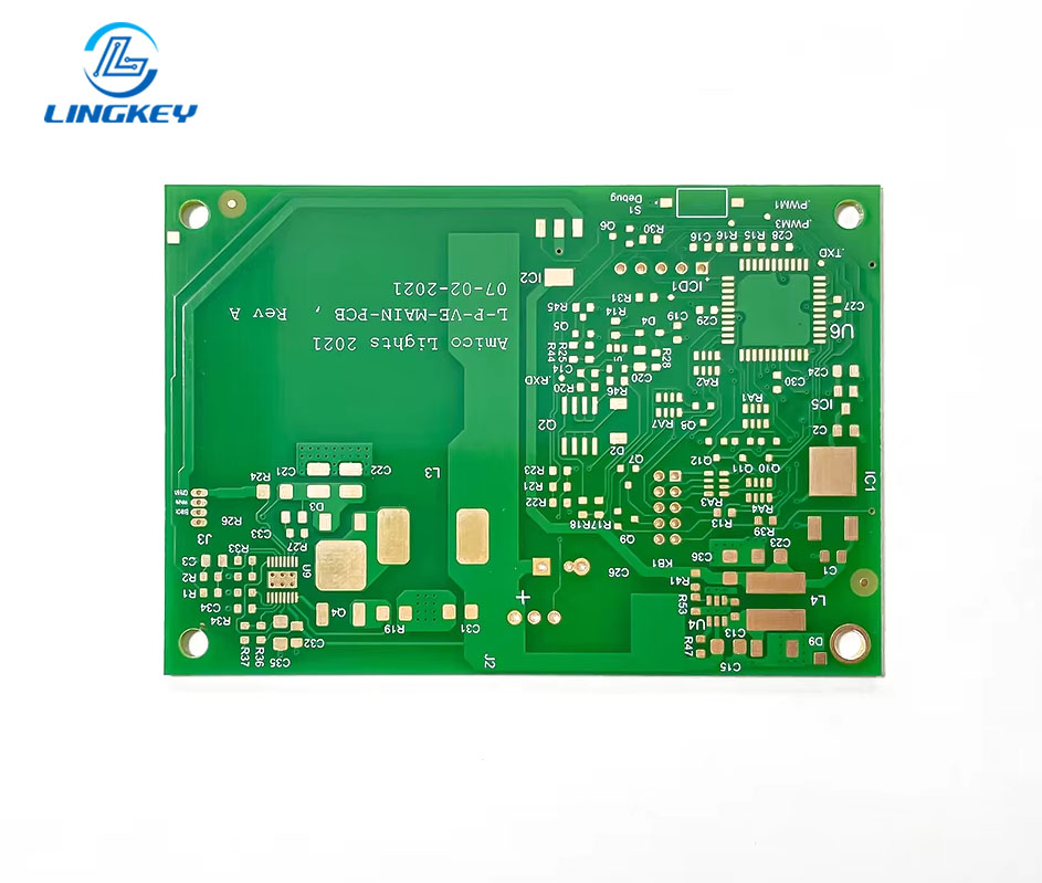
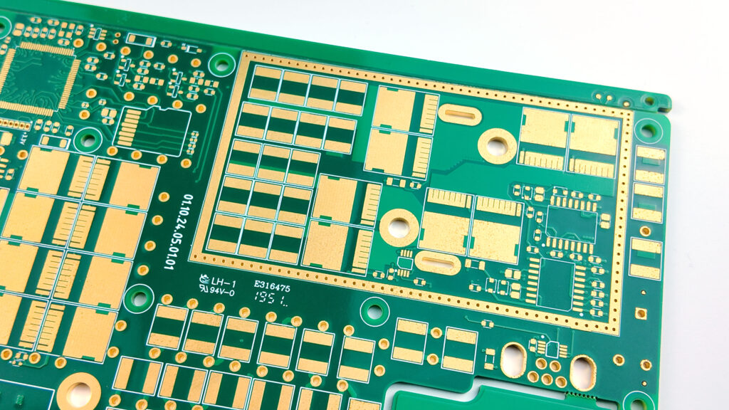
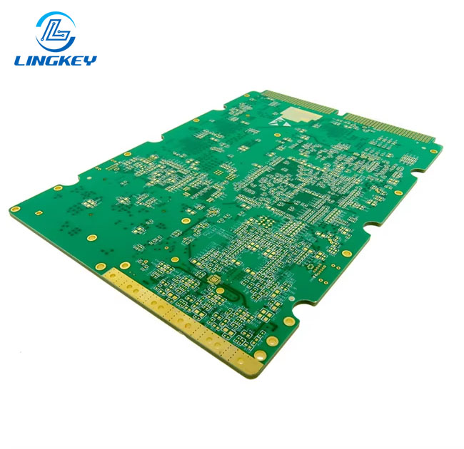
A PCB (printed circuit board) is the standard term worldwide for a bare or – more usually – assembled board. PCB fabrications can be single-sided, double-sided or multi-layered. Multilayer PCBs are widely used in modern electronics as they combine various board layers to achieve high-level functionality and miniaturization.
PCB typically involves:
- Multiple conductive tracesand pads layered with precision for reliable signal transmission.
- Components are soldered onto the PCB—ranging from surface mount to through-hole types.
- Basic manufacturing processallows for scalability, quality, and robust electrical connections across different layers.
PCBA (Printed Circuit Board Assembly) has become a buzzword as PCB is assembled and tested for the end use on every high-end circuit board from smart phones to automotive controllers.
Key Difference Between PWB and PCB
Feature | PWB (Printed Wiring Board) | PCB (Printed Circuit Board) |
Meaning | Bare board, wiring only | Assembled or bare, standard term |
Usage | Pre-assembly, legacy, Japan | Modern, global, after assembly |
Layers | Usually simple (1-2 layers) | Single to many (>20) multilayer PCBs |
Technology | Older, basic | Technology advanced, supports HDI, SMD |
Electrical Connections | Traces only | Full signal, power, ground layers |
Assembly | Not assembled | May or may not be assembled |
PWB vs PCB: Key Differences and Evolution
Historical and Technological Roots
- Difference between PWB: Emphasized the wiring, conductive material, and structure.
- Term PCB: Became universal as circuits, layers, and signal processing needs advanced.
- Process differences:PWB assembly focused on wiring; pcb assembly involves component placement, soldering, and testing.
Multilayer PCBs and Signal Transmission
With the increased complexity of design and manufacturing, there became more layers and complexity inside the board. Multilayer board construction allows signals to be transmitted not only within a layer but also from layer to layer via vias and special stack-ups. Key differences between PWB and PCB include:
- The number of layers (PCBs can be multilayer; PWBs are often single or double-sided)
- The degree of signal transmissionand integration of functional blocks
- The use of miniaturized, SMD packagecomponents and embedded features like antennas
Related Terms for Circuit Boards
As the industry evolved, additional acronyms emerged, each denoting specific assembly stages or practices.
Acronym | Meaning | Context/Usage |
PCB | Printed Circuit Board | Industry standard, global |
PWB | Printed Wiring Board | Pre-assembly, legacy |
PCBA | Printed Circuit Board Assembly | Fully assembled PCB |
CCA | Circuit Card Assembly | Often aerospace, less common |
PCA | Printed Circuit Assembly | Similar to PCBA, US-centric |
PWA | Printed Wire Assembly | Rarest, military/defense |
PB | Printed Board | IPC, generic |
Materials and Structure of PCB and PWB
The heart of any circuit board lies in its structure of PCB and material stack:
- PCB materials: FR-4 (most common), CEM-1, polyimide (flex PCBs), or ceramic substrates for high frequencies.
- Conductive material: Copper, and occasionally gold or silver for specialty applications, is used to createtraces, pads, and planes.
- Different layers: Include power, ground, signal—bonded togetherwith prepreg substances and solidified under heat and pressure.
- Solder mask: Prevents unintentional conduction and oxidation.
- Silk screen: Adds text, orientation, and part information.
Manufacturing and Assembly Process
PCB and PWB Production Workflow
- Design: PCB design software models the different layers of the board, arranging conductive traces for optimum layout.
- Etching circuits: Photoresist, light-exposure, and chemical processes define where conductive materialstays and is removed.
- Drilling: Vias allow signal transmission between layers, while mounting holes secure components.
- Lamination: In multilayer PCBbuilds, layers are stacked and fused.
- Coating: Solder mask and optionally a conformal coatingfor extreme environments.
- Soldering components onto the PCB: Both wave and reflow soldering are used to createrobust electrical connections.
PCBA or PCB assembly is the process of populating the board as the initial PWB is empty. Both quality and repeatability were secured by automatic machines.
Performance, Layers, and Signal Transmission
Modern PCB technology stresses reliability, especially as advanced circuits push boundaries:
- Signal Processing: High-speed circuits need exact layer registration and controlled impedance. PCB typicallyoffers features for optimal signal transmission not possible with legacy PWB approaches.
- Electrical Connections: Vias and plane layers create robust paths for current and signals across different layers.
- Quality Control: Compliance with IPC-A-600 and IPC-A-610 standards is mandatory for critical applications.
Applications of PWB and PCB
The use of PWB and PCB lies in almost every industry today. Historically, because of their simpler design, PWBs were used for applications that required only basic interconnections or more substantial, point-to-point wiring. Now their application is limited to prototyping, repair, and some industrial/specialty markets where a bare board or simple assembly is adequate.
Nevertheless, the electronics industry is mainly influenced by the PCB technology for its capability to provide high integration, high reliability, and miniaturization solutions.PCB and PWB applications cover:
- Consumer Electronics:From smartphones to tablets, dense component integration facilitating advanced functions is ensured by multilayer PCBs.
- Aerospace, Defense, and Automotive Electronics:Strict compliance to standards and the use of advanced materials (conformal coating, ceramic substrates, HDI boards) is mandatory to ensure reliability and safety.
- Medical Devices:Require rigorous QC and error-free signal transmission monitoring and diagnostic equipment.
- Industrial Equipment:Motor controllers, automation, power supplies – all relying on the ruggedness and scalability of the advanced PCB design.
- Telecommunications:The high-frequency PCB materials and multilayer structures, are capable of fast data transfer with embedded antennas.
- Renewable Energy and Power Electronics:High-current paths and intricate thermal management, made possible by modern multilayer PCB manufacturing.
Example Applications
Industry | Typical Board Type | Key Features |
Consumer | Multilayer PCB | Dense, compact, cost-effective |
Aerospace | PCB (often rigid-flex) | Quality, reliability, advanced coating, embedded antennas |
Automotive | PCBA | Signal integrity, thermal management, multi-layer design |
Medical | PCB | Sterile, miniaturized, reliable |
Industrial | PCB/PWB | Custom, rugged, serviceable |
How to Choose: PCB vs PWB?
When navigating terms pwb and pcb in your project, consider:
- Complexity:If your design requires different layers, advanced features, or miniaturization, opt for a multi-layer PCB.
- Standards Compliance:For products that must meet international safety and performance guidelines, “PCB” and, when appropriate, “PCBA” are best for documentation and manufacturing.
- Assembly Needs:A PWB is useful when prototyping or during repair phases, but for mass production, the term PCB is preferred.
- Signal Transmission & Robustness:For high-speed, high-reliability, or precision applications, a multilayer PCB structure is critical.
And keep in mind, the main difference between PWB and PCB isn’t just having components on it, it’s also the level of technology and expectation of standardization within the contemporary electronics industry.
PCB as the Global Standard
Within the world supply chain, pcb is the global language spoken by engineers, component suppliers and manufacturers. The change came about as pcb manufacturing became more complex and as international organisations such as IPC established standards for quality and performance.
Advanced material and multilayer stackup are commonly used in the production of PCBs, making the production of the PCBs faster, they have been standardized and considered as the standard for telecom and datacenter application to consumer gadgets. The flexible, standardized nature of PCB terminology will ensure your docs are understood worldwide, and considered by other technical stakeholders.
In practice, PCB terminology, documentation, and fabrication processes are tailored by manufacturers like LingKey to align with IPC standards for smooth communication throughout design, procurement, and global manufacturing levels.
Best Practices and Care
Cleaning and Maintenance
Long-lasting, high-reliability electronics depend heavily on post-manufacturing cleaning and handling protocols:
- Cleaning:Remove flux residues using isopropyl alcohol or an ultrasonic cleaner to ensure unobstructed, reliable electrical connections.
- Handling:Store boards in moisture-barrier bags, handle with gloves, and avoid bending to protect different layers and prevent micro-fractures.
Understanding Board Layers
Contemporary pcb design can be 4, 6, or even 10+ layers, where each layer has a role – grounding, power delivery, signal transmission optimized. These various layers of the board are laminated together with prepreg and heat, helping in the integration of high-end features and in supporting miniaturization. Designs for building leading-edge electronics make full use of these capabilities.
Industry Services: PCB Production and Assembly
In production, PCB fabricators such as LingKey offer turnkey manufacturing and assembly solutions for rigid, flex, rigid-flex, and HDI board types in IPC-governed environment.
Their offerings include:
- Complete Fabrication:From prototype through full multi-layer production and advanced features like embedded antennas.
- Assembly Services:Automated and manual processes for placing and soldering components onto the PCB.
- Quality Control:Rigorous testing and inspection throughout the manufacturing process.
Frequently Asked Questions: PWB and PCB
What’s the basic manufacturing process for a PCB or PWB?
What is the type of circuit board most often used in modern devices?
Is there a difference between PWB and PCB in practice?
What are terms related to PWB and PCB to be aware of?
Conclusion: The Evolution of Circuit Board Technology
The development of the electronics industry as a whole is reflected in the transformation from PWB to PCB. Over time, the world moved away from primitive point-to-point wiring and rudimentary traces toward multi-layer PCB technologies enabling high — complexity, miniaturized, and dependable electronic modules. The structure of the PCB, Advanced pcb materials and a strong signal over multiple layers make the word PCB is the gold standard for engineers, designers and manufacturers around the world. Knowing what is different, being aware of where process differences lie, and using the right terminology will help you ensure that your projects are founded on clear, quality, and design for the future.
From a production and delivery point of view, the design intent and the terminology and production standards should be preserved throughout the product life cycle, working with an experienced PCB partner as LingKey will help you ensure this. By following IPC-compliant manufacturing and assembly methodologies, robust quality control, and material selection optimized for today’s multi-layer and high-reliability designs, LingKey helps its customers transform PCB designs into solid, scalable, and production-ready hardware for worldwide markets.


