The Best Guide: What Are PCB Test Points (Circuit Board Test Points)?
Introduction to PCB Test Points
When designing a PCB, including test points (TP) — tiny, well-planned access points — can greatly improve your options for circuit board testing, functional testing, debugging and maintenance down the road. Test points are very important: they offer easy access to critical nodes of the circuit, allow both automated and manual testing, and accelerate product development and manufacturing. Whether you are building a simple prototype or high-volume production of a complex integrated circuit assembly, test point placement attention will directly translate into better test and quality assurance outcomes.
In fact, PCB manufacturers such as LingKey usually suggest to consider the test points in the layout design stage for electrical performance, test access and manufacturing process efficiency.
Understanding PCB Test Points
What Is a PCB Test Point?
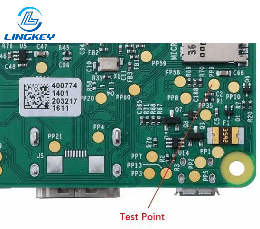
A test point on a PCB is typically a specific pad, via, pin, or loop that provides an access point to the electrical contact for use in circuit board assembly or test. Test points enable engineers, testers, and automated test equipment (ATE) to probe, measure, or stimulate signals at defined locations on the PCB circuit, which is essential to test the full functionality of the board.
The convention of including test points is natural at all stages of PCB manufacturing, from bare board testing to end assembled products. The different testpoint types allow to test contents of board, detect errors, and verify proper soldering and correct component orientation.
The Purpose and Role of PCB Test Points
Test points are used at different stages, from design verification to mass production, for numerous purposes:
- Functional Testing:Confirming that each part of the circuit and the overall board operates as intended.
- Troubleshooting and Debugging:Rapidly isolating problematic nodes or defective components.
- Automated Testing:Enabling access for automated test equipment while executing the in-circuit or flying probe test.
- Quality Assurance:Enabling full inspections and fast error detection to make the final product more reliable.
When carefully sited, test points can provide critical advantages to the manufacturer and the user, particularly in high reliability applications including automotive, medical, and aerospace industries.
Key Uses and Benefits of Implementing Test Points in a Circuit Board Design
Implementing test points on the PCB gives designers, fabricators, and testers distinct technical edges:
- Test the Functionality:In both the design and production phases, test points enable conductive access for measuring voltages, currents, and other electrical quantities.
- Efficient Debugging:Test points make debugging easier, reducing downtime and technician effort.
- Production Efficiency:Automated test machines use the test points to make quick, accurate checks of the circuits, greatly increasing the throughput of the circuit board during assembly.
- Reduced Rework:Early error detection using the test points one can minimize post-production repairs.
- Cost Savings:Test points provide a easy to use test interface without the need to include expensive or bulky components on your board.
Practical Benefits Table
Benefit | Practical Outcome |
Faster Test Cycles | Reduces test/QA time, especially for high production |
Streamlined Debugging | Shortens troubleshooting time through easy access |
Consistent Results | Automated testing ensures standardized quality checks |
Lower Costs | Reduces need for manual rework and inspection |
Enhanced Reliability | Ensures functionality before units leave the factory |
Types of PCB Test Points
Selecting among different test point styles constitutes an important consideration in PCB design and manufacturing. Here are the most common options:
Standard Probe Test Points
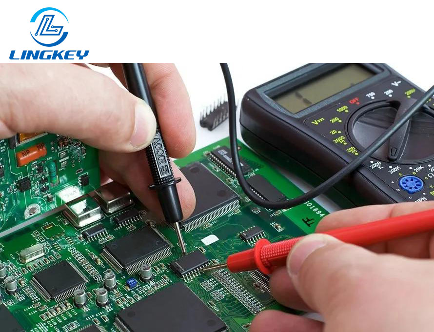
These are plain exposed pads or PTH, on the side of the board, where you can directly connect multimeter leads or benchtop probes.
Surface-Mount Technology (SMT) Test Points
Mainly Utilized for dense count grids they are a small, flat pad that can be accessed by test probes or flying probe testers – machines with moving probes that move around the board to contact each test point.
Through-Hole Test Points
These are robust pins or vias designed for high-reliability connections, in particular adapted for power testing or on multilayer pcbs.
Automated Test Points & Test Nodes
Test points are sized and positioned to be accessible by automated test equipment such as the needles of an ICT fixture or by robotic handlers. PCB design software assists in designating critical nets as test points and the placement of test points are optimized for use in automated fixtures.
Specialized Test Structures
Boards with high-frequency or RF portions may use specialized structures to avoid signal loss or interference.
Core Testing Methods That Use PCB Test Points
The integration of test points is central to several major PCB testing methodologies:
Bare Board Testing
Before assembly, the test points designated for BB tests are utilized to test continuity and insulation between traces and components on the PCB.
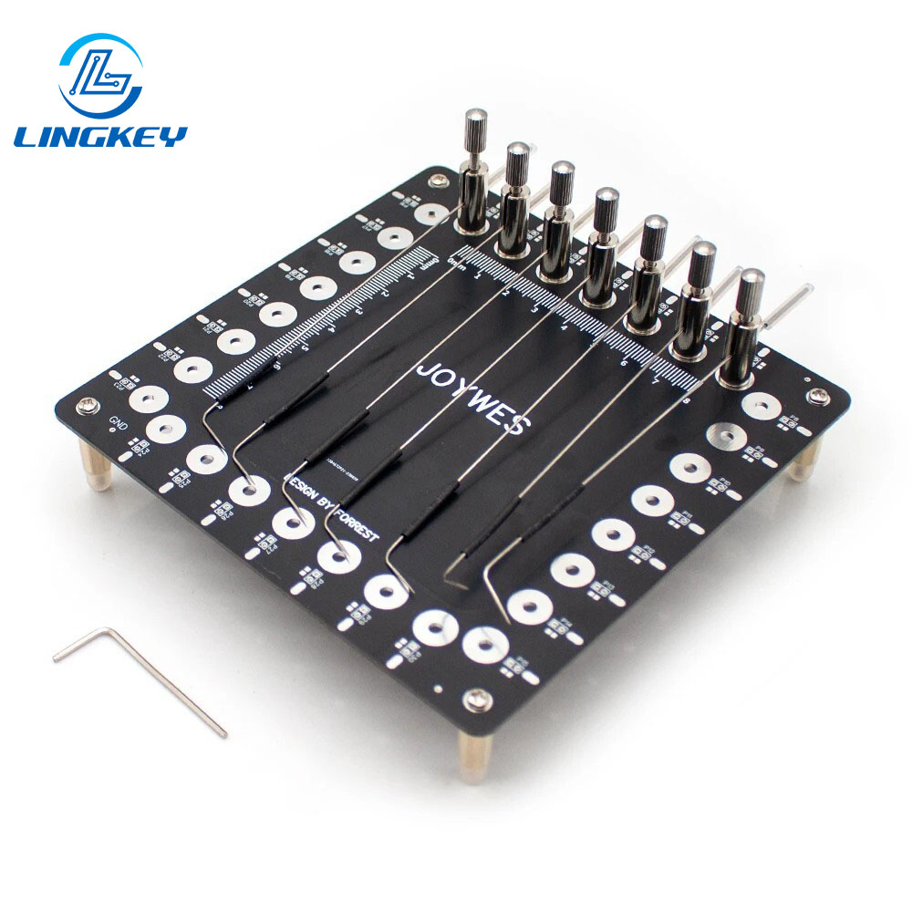
In-Circuit Testing (ICT)
Automated test equipment such as a “bed of nails” fixture is used to make contact with the test points on a populated PCB and verify every electrical connection and component—resulting in enhanced defect detection and production throughput.
Flying Probe Testing (FPT)
Flying probe testers have movable test probes, controlled by software, that move over the test points or nodes and make a gradual contact. This adaptable method is without the need for custom test fixtures, so it is useful for prototyping or when board revisions are frequent.
Designing PCBs with Effective Test Points
The development of testable designs is an important part of contemporary PCB design. Here’s how to place test points for best results:
Test Point Placement and Clearance
- Test points should be evenly distributed across the entire PCB to maximize access and coverage.
- Clearance: Points should be at least 1.27 mm (0.050″) apart to avoid unintentional shorts.
- Ensure access points have no high-profile components blocking them on either side of the board.
Optimal Grouping and Node Access
- Place test points near critical nets—such as power, ground, and commonly failing signal paths.
- Avoid placing test points too close to sensitive nodes of the circuit where interference may degrade performance.
Board Layout Best Practices
- All test points on the PCB should be clearly marked in design files and silkscreen.
- Use of test points in high-density circuits may require staggered or offset arrangements.
- Modern PCB design toolsmake it easier to plan test point locations and check for physical access before fabrication.
Assigning Test Points in PCB Design Tools
Most pcb design software supports specialized routines to optimize test point placement and assignment.
- Set up design rules in the software to reserve nodes or nets as test points.
- Use the tool’s test point manager to verify spacing, coverage, and clearance.
- Review the design’s DFT (Design for Testability) report to ensure all important parts of the board are accessible via test points.
PCB Assembly Processes Using Test Points
Test points make debugging and verification possible at multiple steps of the circuit board assembly process:
In-Circuit Testing (ICT)
During ICT, a fixture brings electrical probes to each assigned test point on the board, allowing rapid simultaneous checks of hundreds of nodes.
Flying Probe Testing
Probes that move—controlled by test software—go to the test point, without requiring a custom fixture. This is particularly useful in prototype runs or uncertain designs.
Advanced & Specialized Types of Test Points
Test points may also include tailored features for advanced PCBs:
- Phosphor bronzespring-loaded test pins for thousands of test cycles.
- Gold or silver-plated contacts that ensure clean, corrosion-free connections even after repeated probing.
- High-frequency structures that minimize signal disruption.
Best Practices for Test Points on PCB Designs
Best practices for test points include:
- Assign critical nets as test points wherever possible.
- Use a consistent, logical numbering or labeling system for easy reference throughout the fabrication and functional testing process.
- Ensure clearance for probe landing to avoid damage during testing.
- Consider test point types to match your testing method—be it manual, automated, or a mix.
- Verify placement with a DFT (Design for Testability) analysis in your chosen PCB design software to ensure all required nodes are accessible and testing coverage is optimal.
Practice | Reason | Benefit |
Assign critical nets as test points | Ensures power, ground, and signal lines are easily accessed | Faster fault detection, comprehensive tests |
Points should be evenly distributed | Prevents cluster-related access issues and testing blind spots | Streamlined access by automated equipment |
Maintain minimum clearance between points | Reduces the risk of accidental shorts and probe misalignment | Improved safety and test accuracy |
Avoid high-density placement near sensitive nodes | Protects high-frequency or analog signals from distortion | Maintains signal integrity |
Place test points on accessible sides | Eases access during both manual and automated testing | Increases efficiency, reduces touch-ups |
Common Mistakes and Limitations with PCB Test Points
Even with experience in the PCB industry, common mistakes are easy to make if diligence is lacking during the layout phase:
- Test point overcrowding: May lead to unintentional bridging or cause test fixtures or flying probe testers not being able to reliably contact each test point.
- Neglecting high-frequency requirements:Close test points may inadvertently influence signal flow or generate parasitic effects which degrade the functionality of the printed circuit.
- Failing to update documentation:If a test point is added, deleted, or changed in the design files it must be updated in the silkscreen layers and assembly instructions.
- Inconsistent assignment:Partial or inconsistent choice about which part of the circuit or which component of the board will have a test point may lead to inadequate coverage.
- Insufficient spacing:The points must be no closer than 1.27 mm apart to be suitable for most contemporary test probes.
Constraints appear when test point planning is an afterthought, or is not applied in the design phase, particularly for high complexity multilayer PCBs or very small form factor designs. In these situations, space is at a premium, and it’s a major challenge to balance accessibility with functionality and signal integrity.
Applications and Challenges of PCB Test Points
Test points are essential in every sector that uses printed circuits:
Key Applications
- Consumer electronics:Testing points enable fast functional testing and quality checking of devices ranging from cell phones to game machines.
- Automotive and aerospace:The high reliability requirement implies that each node of the circuit can be designated as a test point for comprehensive electrical and environmental testing.
- Medical devices:The standard is for validated assembly, with the test points conclusively demonstrating the unit is good to go.
- Industrial automation:Such maintenance and reprogramming will require that access points be provided, able to tolerate frequent contact.
Challenges
- High-density layouts:Packing in enough test points for a PCB circuit while maintaining clearance is still an issue.
- Mixed-signal and high-frequency designs:Here, the presence, location, and size of test points must be carefully weighed against potential interference.
- Prototype vs. production boards:Prototyping can allow more freedom in test point placement, but in production, test points are optimized for speed and real estate is minimized.
Frequently Asked Questions (FAQ) About PCB Test Points
How do I place test points most effectively?
What are the different test point types I should consider?
Why is it important that test points should be evenly distributed?
How do flying probe testers improve test?
Do test points impact the functionality of my printed circuit board?
Conclusion — The Bottom Line on PCB Test Points
The use of test points in PCB design is essential for today’s electronics. Correct test point location, spacing, and documentation improves circuit board assembly, manufacturing, and quality control, as well as functional testing, debugging, and maintenance. For prototyping, high-volume production, or field troubleshooting, test points provide instant, repeatable access to any portion of the circuit, guaranteeing the performance and reliability your applications require.
With the support of capable production partner such as LingKey, good PCB test points allow the design intent to be manifested into stable testing, quicker verification and regular product performance in quantity.


